Understanding Enhancement-mode MOSFETs: Symbol, Types, and Advantages
2024-06-04
39345
Catalog

Figure 1: Enhancement-Mode MOSFETs
Introduction to Enhancement-Mode MOSFETs
Enhancement-mode MOSFETs are integral to modern electronics, known for their compact design, efficient power management, and ease of manufacturing. These attributes make them ideal for dense and complex circuit architectures where space and energy efficiency are required.
An enhancement-mode MOSFET remains non-conductive when the gate-to-source voltage (Vgs) is zero, classifying it as 'normally off'.
Activation occurs with a positive Vgs for NMOS or a negative Vgs for PMOS. This voltage induces an inversion layer at the semiconductor-oxide interface, forming a channel that allows charge carriers (electrons for NMOS and holes for PMOS) to flow from the source to the drain. The ability to enhance channel conductivity on demand with a gate voltage is the conducted of enhancement-mode MOSFETs, setting them apart from depletion-mode MOSFETs, which are "normally on" and can conduct without gate voltage.
Enhancement-mode MOSFETs excel in minimizing power consumption. When off, they use very little power, a fundamental advantage for power-sensitive applications like portable electronics and power supply design. Their manufacturability using modern semiconductor technologies makes them cost-effective and scalable for both high-volume consumer electronics and specialized industrial applications.
Enhancement MOSFETs Symbol
The symbol for an enhancement MOSFET in electronic diagrams provides fundamental clues about its operational mode and structure. It features a broken or dashed line from the gate to the channel, unlike the continuous line in depletion-mode MOSFET symbols. This broken line signifies the 'normally off' nature of enhancement-mode MOSFETs, indicating that a conductive channel forms only with an appropriate gate-to-source voltage.
N-Channel Enhancement-Mode MOSFETs
In N-channel enhancement-mode MOSFETs, the substrate is typically made of p-type semiconductor material. A thin layer of silicon dioxide (SiO2) acts as the gate insulator above this substrate, with a metallic gate electrode positioned on top. When a positive voltage is applied to the gate relative to the source, an electric field is created, attracting electrons to the SiO2 interface and forming an n-type conductive channel between the source and drain terminals. The channel's conductivity increases with the applied voltage, allowing control over the electron flow through the device.
P-Channel Enhancement-Mode MOSFETs
In P-channel enhancement-mode MOSFETs, the substrate consists of n-type semiconductor material. Applying a negative voltage to the gate relative to the source generates an electric field that repels electrons from the silicon surface beneath the gate and attracts holes, forming a p-type conductive channel. This setup enables the movement of holes from source to drain, allowing current to flow in the opposite direction to that in N-channel MOSFETs.

Figure 2: N-Channel Enhancement-Mode MOSFETs
Design Principles of the n-Channel Enhancement-Mode MOSFET (NMOS)
The n-Channel Enhancement-Mode MOSFET, or NMOS, is built on a p-type substrate, which provides both structure and operational support. This substrate houses two critical n-type regions: the source and the drain. These regions enable the flow of electrons, forming the current through MOSFET.
There is a thin layer of silicon dioxide (SiO2) between the source and the drain. SiO2 is chosen for its high dielectric strength and reliability, acting as an insulator to prevent unintended current flow when the device is off. Above this oxide layer is the gate electrode, usually made of metal. The gate is required for controlling the MOSFET's operation. When voltage is applied to the gate, an electric field changes the device's conductivity.
A key characteristic of the NMOS is that it does not have a native conductive channel between the source and drain when in its default state. This design makes it an enhancement-mode MOSFET, requiring a specific gate voltage to form a conductive channel. Adjusting the gate voltage allows the device to switch between on and off states, allowing precise control in electronic circuits.
Connections to the source, drain, and substrate are carefully designed to ensure low resistance and high signal integrity. The lack of a pre-formed channel means the NMOS relies on external voltage to conduct, offering enhanced control over its operation. This feature is handy in digital electronics where binary switching is required.
NMOS with Gate-to-Source Voltage (Vgs= 0)
When the gate-to-source voltage (Vgs) is set to zero, the NMOS transistor operates as a three-terminal device with distinct electrical properties. This condition is required to minimize unintended interactions between the terminals, thus enhancing the device's reliability and performance in various circuits.
With Vgs at zero, there is no potential difference between the gate and the source. This lack of potential difference prevents the formation of a conductive channel between the source and the drain, keeping the NMOS in a non-conductive or 'off' state. This off-state matters for switching applications in digital circuits.
To further prevent leakage currents between the drain and source, the NMOS includes built-in protection mechanisms. The source and drain are connected to the p-type substrate, forming p-n junctions. These junctions act as reverse-biased diodes when the transistor is off. The reverse biasing effectively blocks the flow of charge carriers, preventing unwanted current flow.
This behavior is different from Junction Field-Effect Transistors (JFETs) and depletion-type MOSFETs. In those devices, a nonzero drain current (Id) can be observed even when Vgs is zero because of a naturally formed channel. In contrast, the NMOS requires a positive Vgs to create a channel, highlighting a key operational difference urgent for applications needing precise control over the transistor's on and off states.
NMOS with Positive Gate-to-Source Voltage (Vgs> 0)
When the gate-to-source voltage (Vgs) is positive, the NMOS transistor changes significantly in its conductive state, which is valuable for its role in amplifying and switching.
When a positive Vgs is applied, an electric field forms across the gate electrode. This field affects the p-type substrate underneath by repelling holes, which are the primary carriers in the substrate. As holes are pushed away from the substrate-SiO2 interface, a depletion region forms, lacking mobile charge carriers and increasing resistance in this layer.
As Vgs increases further, the electric field becomes strong enough to attract electrons from the n-type source and drain regions. These electrons gather at the boundary of the depletion region within the SiO2 layer, forming an inversion layer. This inversion layer converts the behavior of the semiconductor at the interface from p-type to n-type, creating a conductive pathway.

Figure 3: Channel Formation in the Enhancement-mode NMOS
When a voltage is applied across these terminals, the newly formed n-type channel allows current to flow between the source and drain. The strength of the electric field in the gate's structure modulates the conductivity of this channel, thereby controlling the current magnitude.
A significant component of this process is the threshold voltage (VT), the minimum gate voltage needed to form the conductive channel. VT depends on several factors: the substrate's doping concentration, the SiO2 layer's thickness and dielectric constant, and the transistor's physical dimensions.
NMOS with Negative Gate-to-Source Voltage (Vgs < 0)
The enhancement-mode NMOS transistor behaves differently under negative gate-to-source voltages compared to depletion-mode NMOS or Junction Field-Effect Transistors (JFETs). While depletion-mode devices can either enhance or deplete the carrier concentration in the channel with a negative gate voltage, the enhancement-mode NMOS has more restrictive dynamics.
For enhancement-mode NMOS, a negative Vgs cannot initiate conduction. This is because the device has no pre-existing conductive channel and relies on positive gate voltage to induce one. When Vgs is negative, the electric field between the gate and the substrate repels electrons from the gate region, reinforcing the depletion region and preventing the formation of a conductive channel. Thus, the transistor remains off.
This characteristic defines the NMOS as an 'enhancement-mode' device. It highlights the device's need for positive gate voltage to enhance electron concentration in the channel. This behavior counts for digital logic applications where a distinct and reliable off-state is needed to prevent unwanted current flow and ensure clear logical states.
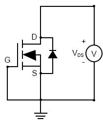
Figure 4: Voltage Application Between Drain and Source
Voltage Application Between Drain and Source
Understanding the interaction between the drain-source voltage (Vds) and the gate-source voltage (Vgs) is useful in controlling the current flow and operation of an NMOS transistor, especially when a positive voltage is applied between the drain and source.
• Low Vds: Ohmic Region
Initially, with low Vds, the NMOS acts like a variable resistor. The transistor operates in the "ohmic" or "triode" region, where the channel remains open and unpinched. In this region, the drain current (Id) varies linearly with Vds. Vgs mainly control the conductivity of the channel. A higher Vgs increases electron concentration in the channel, decreasing its resistance and allowing more current to flow.
• Increasing Vds: Transition to Saturation
As Vds increase, the voltage drop along the channel affects electron distribution. When Vds reaches a critical point, equal to or greater than (Vgs - VT), the channel near the drain starts to narrow or "pinch off." This marks the transition from the ohmic region to the saturation region. In saturation, the channel near the drain effectively closes, restricting the active channel region to the source end.
• Saturation Region: Stable Current
In the saturation region, Id reaches a maximum value, called the saturation current, which remains stable even if Vds increases further. This stable current output is necessary for applications where NMOS is used as a switch or amplifier, as it maintains consistent performance at different drain voltages.
Drain Characteristic and Transfer Curve in NMOS Transistors
The drain characteristic and transfer curve are key to understanding how enhancement-mode NMOS transistors manage voltage and current. These curves provide insight into the device's behavior under different operating conditions.

Figure 5: Drain Characteristic and Transfer Curve
The core of NMOS operation lies in its volt-ampere characteristic, like other field-effect transistors (FETs). For gate-to-source voltages (Vgs) less than or equal to the threshold voltage (VT), the NMOS has very high resistance, effectively blocking current flow from drain to source. This defines its enhancement mode, where a Vgs exceeding VT is required to turn the transistor 'on' and allow conduction.
Once Vgs exceeds VT, the channel resistance decreases, increasing the drain current (Id). This relationship is represented in the transfer curve, which plots Id against Vgs starting from VT. The curve shows how Id rises with increasing Vgs, highlighting the gate voltage's control over the current through the device.
High drain-to-source voltages (Vds) can stress the channel, especially near the drain where the electric field is strongest. This stress can cause channel breakdown, typically due to avalanche breakdown in the space-charge region at the drain end. During avalanche breakdown, the strong electric field generates electron-hole pairs, increasing current significantly and potentially damaging the transistor.

Figure 6: P-Channel Enhancement-Mode MOSFET (PMOS)
Design Principles of P-Channel Enhancement-Mode MOSFET (PMOS)
The P-Channel Enhancement-Mode MOSFET, or PMOS, is designed as a mirror image of the n-Channel MOSFET (NMOS), a key aspect of its operation and use in electronic circuits, especially where complementary functions are needed.
In a PMOS transistor, the substrate is made of n-type semiconductor material, unlike the p-type substrate in an NMOS. This n-type substrate is paired with p-type regions for the source and drain, facilitating the flow of holes, the charge carriers in PMOS, as opposed to electrons in NMOS.
The operation of a PMOS transistor starts by applying a negative gate-to-source voltage (Vgs). This negative voltage inverts the carrier concentration under the gate, creating a conductive p-channel. As the magnitude of the negative Vgs increases, more holes gather in the channel area, enhancing conductivity between the source and drain.
In contrast to an NMOS, where a positive Vgs induces a channel, a PMOS requires a negative Vgs for conduction. The direction of current flow in a PMOS is also reversed; current flows from source to drain are driven by the movement of holes, which are positive charge carriers.
The PMOS's design complements the NMOS, extending the versatility of MOSFET technology. This complementary nature plays a role in Complementary Metal-Oxide-Semiconductor (CMOS) technology, foundational in modern digital circuitry. CMOS technology benefits from higher efficiency and lower power consumption because only one type of transistor (either NMOS or PMOS) conducts at a time, minimizing current draw during the switch-off phase.
Drain Characteristic and Transfer Curve of the PMOS
The PMOS, or P-Channel MOSFET, operates with dynamics opposite to those of the NMOS, especially regarding how the gate-to-source voltage (Vgs) influences conductivity.

Figure 7: Drain Characteristic and Transfer Curve of the PMOS
In a PMOS device, increasing the negative Vgs enhances the concentration of holes (positive charges) in the semiconductor region beneath the oxide layer. This increase in hole concentration directly boosts conductivity across the channel formed between the source and drain terminals.
The transfer curve of the PMOS, which plots the drain current (Id) against Vgs, shows that Id increases as Vgs becomes more negative, moving past the threshold voltage (VT). For a PMOS, VT is the minimum gate voltage needed to create a conductive channel with holes. This characteristic curve is a mirror image of the NMOS's curve, reflecting the PMOS's operation with inverted voltage polarities and charge carriers.
In CMOS circuits, the complementary operation of these devices is utilized to great effect. The PMOS transistors efficiently modulate conductivity with changes in gate voltage. In CMOS configurations, using both types of transistors allows for a design where one type conducts while the other is off, enhancing circuit efficiency and reducing power consumption. Minimal current flows through the circuit except during the switching phase, when both transistors momentarily conduct.
Operational Mechanics of Enhancement MOSFETs
Enhancement MOSFETs operate based on the gate-to-source voltage (VGS). In its default state, with VGS at zero, the device remains non-conductive, or 'normally off'.

Figure 8: Characteristics of Enhancement MOSFETs
The activation begins when a gate voltage is applied. For NMOS, a positive gate voltage relative to the source is required, while PMOS needs a negative gate voltage. This voltage creates an electric field through the silicon dioxide or similar dielectric layer, impacting the semiconductor material beneath the gate.
In NMOS, a positive VGS repels holes (majority carriers in the p-type substrate) and attracts electrons (minority carriers) to the silicon dioxide interface. This accumulation of electrons forms an n-type inversion layer, creating an n-channel that allows current to flow from the source to the drain. In PMOS, a negative VGS repels electrons and attracts holes, forming a p-channel.
The formation of these channels significantly reduces the resistance between the source and drain. The channel's conductivity depends on the number of charge carriers (electrons or holes) in the channel. The greater the gate voltage, the stronger the electric field, attracting more carriers and enhancing conductivity. The ability to modulate channel resistance via gate voltage is a fundamental advantage of enhancement MOSFETs.
Applications of Enhancement Type MOSFETs
Enhancement Type Metal-Oxide-Semiconductor Field-Effect Transistors (E-MOSFETs) are central to modern electronics due to their versatile functionality. Their high input impedance and quick response to input signal changes make them excellent amplifiers. This capability is required for boosting weak signals in audio devices and communication systems, where maintaining signal integrity is required.

Figure 9: E-MOSFETs for Power Switching
In power switching, E-MOSFETs excel by efficiently toggling between on and off states with minimal gate voltage adjustments. This enhances power management in devices ranging from computer power supplies to industrial machines, improving performance while reducing energy costs.
For memory storage, E-MOSFETs ensure reliable data retention, which is ideal for devices such as USB drives and advanced solid-state drives (SSDs). These components are key to the robust architecture of modern computing systems.
E-MOSFETs also play an imperative role in inverter circuits, which convert direct current (DC) to alternating current (AC). Their reliability and efficiency are key in applications like solar power setups and uninterruptible power supplies (UPS), ensuring consistent power delivery. Furthermore, their use in power electronic circuits supports the development of compact, high-efficiency integrated circuits (ICs) found in various gadgets, broadening functionality and enhancing performance.
In motor control, E-MOSFETs precisely regulate the speed, direction, and torque of motors in both industrial and consumer applications, including electric vehicles and automated production lines. Their efficiency is key to optimizing performance in these areas. E-MOSFETs are also adaptable for use in digital controllers and systems, managing logic operations and processing tasks fundamental for advanced digital communications and computing functions.
E-MOSFETs are present in everyday tools like calculators and analog switches, facilitating complex mathematical calculations and data handling to ensure user-friendly and reliable devices. In radio systems, E-MOSFET-based oscillators provide stable frequencies integral for consistent communication.

Figure 10: E-MOSFETs for Car Audio Setup
Finally, in sound systems ranging from car audio setups to large sound reinforcement systems, E-MOSFETs manage power distribution and enhance signal amplification. This ensures high-quality audio output, delivering clear and robust sound for both personal and public settings, and creating immersive audio experiences.
Pros and Cons of Enhancement MOSFETs
Pros of E-MOSFETs
Voltage-Controlled Operation:SFETs are controlled by voltage, not current, leading to minimal current draw from the input source. This reduces power consumption and signal loss, beneficial for battery-operated and low-power devices. Apart from that, their high input impedance means they exert minimal load on the preceding circuit stage, preserving signal integrity and enhancing overall circuit performance.
Compact Size:The small size of E-MOSFETs allows for the design of compact, lightweight electronics such as smartphones, wearables, and portable medical devices.
High Reliability and Robustness:The silicon dioxide layer insulates the gate from the substrate, providing excellent electrical isolation. This contributes to the high reliability and robustness of E-MOSFETs, ensuring stable operation across various conditions. Plus, E-MOSFETs can switch at high speeds with great precision, making them ideal for applications requiring rapid switching, such as digital logic circuits, RF amplifiers, and power converters.
Low On-Resistance:When on, E-MOSFETs exhibit low on-resistance, allowing efficient current conduction with minimal power loss. This efficiency is fundamental in power electronics, where energy conservation and thermal management are required.
Cons of E-MOSFETs
Complex Biasing Requirements: E-MOSFETs generally require more complex biasing circuits compared to other transistors like BJTs (Bipolar Junction Transistors). This can complicate integration into electronic systems and may require additional components and design considerations.
Temperature Sensitivity: E-MOSFET performance can be affected by temperature variations. High temperatures can alter the threshold voltage (Vt) and other operational parameters, potentially impacting performance and stability.
Cost Considerations: E-MOSFETs can be more expensive to manufacture than other types of transistors, which can impact the overall cost of the electronic system.
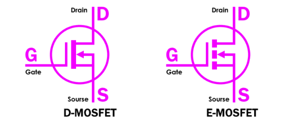
Figure 11: D-MOSFET vs. E-MOSFET
Enhancement MOSFET vs. Depletion MOSFET
|
|
Enhancement MOSFET (E-MOSEFT) |
Depletion MOSFET (D-MOSFET)
|
|
Default State |
"normally off" and need a positive gate voltage to conduct |
"normally on" and conduct at zero gate voltage |
|
Control Mechanism |
require a positive gate voltage to induce a channel, providing clear on/off control suitable for digital switching |
modulate an existing channel, offering broader control for both switching and continuous conduction applications |
|
Application Suitability |
excel in high-speed switching and digital applications due to their rapid response to gate voltage changes |
better suited for applications needing stable current flow and analog signal amplification |
Chart 1: Difference Between Enhancement MOSFET and Depletion MOSFET
Conclusion
The study of enhancement-mode MOSFETs (E-MOSFETs) reveals their integral role in modern electronics, driven by their inherent efficiency, compactness, and robust performance under varied operational demands. From digital logic circuits to power management systems, E-MOSFETs are required to optimize the performance and energy efficiency of an array of devices. The article has highlighted the subtle yet needed differences between n-channel and p-channel MOSFETs, elaborating on their operational dynamics, which are perfect for applications like CMOS technology where complementary functionalities are leveraged. Moreover, the discussion of their advantages juxtaposed with challenges like complex biasing requirements and temperature sensitivity, provides a comprehensive understanding of their application scope and limitations. This analysis not only enhances our understanding of MOSFETs but also underscores their significant impact on the development of innovative, reliable, and efficient electronic systems.
Frequently Asked Questions [FAQ]
1. Why is enhancement MOSFET preferred?
Enhancement MOSFETs are preferred due to their high efficiency and power-handling capabilities. Unlike depletion MOSFETs that are normally on, enhancement MOSFETs are normally off, meaning they require a voltage on the gate to turn on. This characteristic makes them useful in circuits that require low power consumption when in the off state, as well as in applications where switching control is required, such as in power supplies and motor controls.
2. How do I know if my MOSFET is an enhancement?
To determine if a MOSFET is an enhancement type, check its datasheet for the threshold voltage (Vth). If the device requires a positive gate-source voltage (VGS) to turn on, it is an enhancement MOSFET. This is opposed to a depletion type, which can be conducted even when the gate-source voltage is zero or negative.
3. How does an enhancement type MOSFET differ from BJT?
An enhancement type MOSFET differs from a Bipolar Junction Transistor (BJT) in several key ways:
Control: MOSFETs are voltage-driven, meaning they require a voltage at the gate to control the flow of current through the channel. BJTs are current driven, needing a current at the base.
Power: MOSFETs generally consume less power during operation since there is no continuous gate current, unlike the base current in BJTs.
Switching Speed: MOSFETs typically have faster switching speeds due to the absence of charge storage issues that affect BJTs.
4. Do MOSFETs use AC or DC?
MOSFETs can be used with both AC and DC signals. For DC applications, they function as switches or amplifiers. In AC applications, they are used in converters and inverters. The ability to operate with both types of signals makes them versatile in various electronic circuits.
5. Are MOSFETs voltage or current driven?
MOSFETs are voltage-driven devices. The operation of a MOSFET depends primarily on the voltage applied to the gate terminal, which controls the conductivity of the channel between the source and the drain, with no need for a significant continuous current to flow into the gate.
6. What is the enhancement mode MOSFET equivalent to?
The enhancement mode MOSFET is equivalent to a normally open switch in electronic circuits. It remains off when there is no voltage applied to the gate, and it turns on when a sufficiently positive voltage is applied, allowing current to flow through the channel.
7. What is the conducting channel in an enhancement mode MOSFET?
In an enhancement mode MOSFET, the conducting channel is formed when a positive voltage is applied to the gate relative to the source. This voltage induces a channel of charge carriers (electrons for n-channel, holes for p-channel) under the gate, which allows current to flow through the device between the drain and the source terminals. The strength and conductivity of this channel can be controlled by the gate voltage, allowing for precise control over the current flow.
function test. The highest cost-effective products and the best service is our eternal commitment.
Hot Article
- LM358 Dual Operational Amplifier Comprehensive Guide: Pinouts, Circuit Diagrams, Equivalents, Useful Examples
- Are CR2032 and CR2016 Interchangeable?
- Understanding the Differences ESP32 and ESP32-S3 Technical and Performance Analysis
- BC547 Transistor Basics: Pinout, Application Circuits, Alternative/Complementary Models
- Choosing the Right Battery: A Guide to AG4, LR626, LR66, 177/376/377, SR626, and SR626SW Equivalents
- NPN vs. PNP: What's the Difference?
- esp32 vs stm32: which microcontroller is better for you?
- What Is a MOSFET and How It Works?
- Electrical Relay Basic: Working Operation, Types and Uses
- PNP Transistors: Structure, Working Principle and Application
 Explore the Principles, Symbols, and Applications of Depletion-Mode MOSFETs
2024-06-05
 System on Chip (SoC) vs Single Board Computer (SBC): Key Differences and Applications
2024-06-03
Hot Part Number
 CGA5L3X7S2A155M160AB
 C3225JB2A155K200AB
 CGA8P1C0G3F331K250KA
 12065A332KAT2A
 06035A130CAT2A
 SMAJ7.0A
 MAX14983EETJ+
 V110B24T150BG
- V300B48H250BN
 BSC050N03LSGATMA1
- RT0805BRD073K6L
- KD224503
- RS1D
- LT323AT#PBF
- ADG438FBRZ
- OPA548FKTWT
- AD817AR-REEL
- MM74C912N
- MC1489ADR2
- STA8090FG
- AD5410AREZ
- NC7SZ157P6X
- TLC27L4CN
- ST62T25CB6
- ADG5208FBRUZ
- XA2C256-8VQG100Q
- AD558-6482
- AD7240JP
- BD82C602SLJKG
- CAT5221JI-10
- IDT7014S12JG8
- KFM1216Q2B-VEB8
- LC87F7932BVU-SQFP-H
- LM2711MTADJX/NOPB
- MC100EL57D
- ML6652EH
- PW106-10
- SCC2692AC1A44G
- STC12C5406AD-35I-SOP20
- THGBM4G6D2HBAIR
- UPD70F3015BGC-8EU-A
- ES8680CSC
- RCAMP0514M.TBT
- S1L1491X01-T0
- LCU032420
- LM2575GR-ADJ
- 6ES7516-3FN02-0AB0
- TEN30-4813WI
- MT42L128M64D2LL-25