Voltage Multipliers: Doublers, Triplers, Quadruplers and Their Impact on Modern Electronics
2025-07-14
32431
Catalog
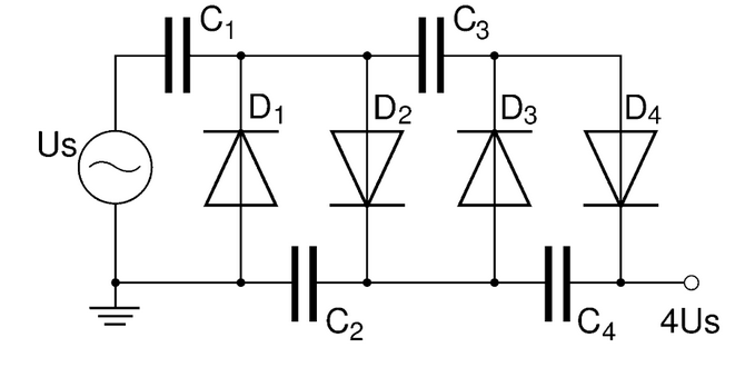
Figure 1. Voltage Multiplier
What is a Voltage Multiplier?
A voltage multiplier is an electrical circuit that uses diodes and capacitors to convert a lower AC voltage into a much higher DC voltage, without using a transformer. These circuits work by stacking voltage in stages, where each stage incrementally adds the peak input voltage. Voltage multiplier circuits are used to increase voltage levels without the need for heavy transformers.
Calculation of Output Voltage
Figure 2. Output Voltage Diagram
To design a voltage multiplier that meets specific voltage needs, calculating the output voltage is needed. The output voltage (Vout) of a voltage multiplier is determined using a simple formula:
In this formula, Vin is the peak input AC voltage, and 𝑁 represents the number of doubling stages in the multiplier. Each stage effectively doubles the voltage, progressively increasing the input voltage across the stages.
To meet different voltage and performance needs, several types of voltage multipliers have been developed. Each type has its own way of increasing voltage and is used in different situations based on size, efficiency, and output requirements. Let’s discuss below:
Half-Wave Voltage Doubler

Figure 3. Half-Wave Voltage Doubler
A half-wave voltage doubler is an electronic circuit that produces an output voltage approximately twice the peak value of the input AC voltage. It achieves this using two diodes, two capacitors, and an alternating current power source. The circuit is widely used in low-current applications where compact, transformerless voltage multiplication is needed.
Circuit Operation and Waveform
The half-wave voltage doubler works using two diodes and two capacitors. During the positive half cycle of the AC input, the first diode conducts and charges the first capacitor to the peak input voltage. At the same time, the second diode is off.
In the negative half cycle, the polarity reverses. The second diode now conducts, and the voltage from the first capacitor adds to the AC input. This combined voltage charges the second capacitor to roughly twice the input peak voltage.
Once charged, the second capacitor holds this higher voltage and powers the load if connected. This process repeats every AC cycle, allowing the circuit to maintain a near-constant doubled DC output.
The output resembles that of a half-wave rectifier but with twice the voltage. However, since charging only happens on one half of the AC cycle, the output contains ripple, which varies depending on the load and capacitor size.
Advantages and Disadvantages
|
Advantages |
Disadvantages |
|
Simple method for generating high voltage
from lower AC input |
Produces significant ripple in the output
voltage |
|
Avoids the need for bulky transformers |
Poor voltage regulation, especially under
load |
|
Compact and low cost |
Output drops when the capacitor
discharges |
|
Ideal for low-current applications |
Power is delivered only during one half
of the AC cycle, reducing efficiency |
|
Excellent learning tool for understanding
diode and capacitor behavior in voltage multipliers |
Not suitable for high-power applications |
Full-Wave Voltage Doubler

Figure 4. Full-Wave Voltage Doubler
A full-wave voltage doubler is used to increase the peak voltage of an AC input. Instead of relying on a high-turns-ratio transformer, this circuit uses two diodes, two capacitors, and an alternating current (AC) source to double the voltage at the output. The key advantage of this design is that it utilizes both halves of the input AC waveform, allowing for efficient voltage doubling with minimal components.
Circuit Operation and Output Characteristics
During the positive half cycle of the AC input, the voltage rises toward its peak value, Vm. Diode D1 becomes forward biased and conducts current, charging capacitor C1 to Vm. At this point, diode D2 remains reverse biased and blocks current, so capacitor C2 does not charge.
In the negative half cycle, the input polarity reverses. Diode D2 is now forward biased and allows current to flow, charging capacitor C2 to Vm. Diode D1 becomes reverse biased and blocks current, so C1 retains the charge it stored earlier. This alternating behavior continues with each cycle, allowing both capacitors to charge to the peak input voltage.
The output voltage is taken across both capacitors in series. Since each holds Vm, the total output is approximately 2Vm. If no load is connected, the output remains steady. When a load is applied, the voltage drops slightly due to capacitor discharge and component losses.
Unlike half-wave doublers that use only one half of the waveform, this approach captures energy from the entire input signal. The result is a more stable and efficient DC output, nearly double the peak AC input.
DC Voltage Doubler Circuit

Figure 5. DC Voltage Doubler Circuit
A DC voltage doubler circuit increases the peak AC input voltage to produce a higher DC output, typically twice the original peak value. This basic configuration is known as a half-wave voltage doubler, because it utilizes only one half-cycle of the AC waveform for charging, similar to a half-wave rectifier. It offers a cost-effective way to generate higher voltages without relying on a large or expensive transformer.
The circuit uses two diodes (D1 and D2) and two capacitors (C1 and C2). It works by storing and combining voltage from different phases of the AC input cycle. During the negative half-cycle, D1 conducts and charges C1 to the peak input voltage (Vp), while the positive half-cycle turns on D2, enabling C2 to charge to nearly 2Vp by stacking the input voltage onto the stored voltage in C1.
Output Voltage and Ripple Behavior
The output across C2 delivers the doubled voltage to the load. However, this output builds gradually over several input cycles and is not instantly stable. Because the circuit charges C2 only once per cycle, the output contains noticeable ripple at the same frequency as the AC input. This behavior is similar to a half-wave rectifier and may require additional filtering for sensitive electronics.
To ensure safe operation, capacitor C2 should have a voltage rating of at least twice the peak input. This prevents damage and extends the lifespan of the component.
Benefits of Using a Voltage Doubler
Voltage doubler circuits provide an efficient solution for generating high DC voltages from low AC inputs. They eliminate the need for high-voltage transformers, making them ideal for compact or cost-sensitive designs. These circuits are especially useful in low-current applications where space and budget are limited.
The design is flexible. By reversing the diodes and capacitors, you can produce a negative voltage output. You can also cascade multiple stages to build voltage triplers, quadruplers, and higher-order voltage multipliers, allowing further voltage increases in fixed steps.
Limitations of Using a Voltage Doubler
Low current capability. The output voltage drops quickly when driving low-resistance loads. For best results, use the circuit with high-resistance loads, typically 100k ohms or greater. Also, due to its half-wave design, the output ripple can be significant. If smooth DC is required, additional filtering components are necessary.
Building on the same principles as the voltage doubler, a DC voltage tripler circuit further extends this concept to achieve even higher output voltages, making it a valuable option when a greater voltage boost is required without using complex or bulky components.
DC Voltage Tripler Circuit
A DC voltage tripler circuit converts an AC input into a higher DC voltage—specifically, about three times the peak value of the input waveform. This design is a type of half-wave voltage multiplier, meaning it relies primarily on one half-cycle of the AC input for charge transfer, similar to the half-wave doubler circuit. It extends that basic topology by adding one more diode-capacitor stage, enabling higher voltage output without a bulky transformer.

Figure 6. DC Voltage Tripler Circuit
In the circuit shown above, the design combines one full-wave doubler section with an additional half-wave stage. The left half of the image shows the actual electrical layout, while the right side illustrates its modular structure, broken down into a half section and a full section for clarity.
The circuit uses three diodes–D1, D2, and D3—and three capacitors—C1, C2, and C3. These components work together in response to alternating half-cycles of the AC input signal. During the negative half-cycle, diode D3 conducts and allows capacitor C3 to charge to the peak voltage of the input, labeled as Vp. When the input transitions to the positive half-cycle, diode D1 becomes forward-biased. It allows capacitor C1 to charge to 2Vp by stacking its voltage on top of the charge already held by C3. Diode D2 then passes this combined voltage to capacitor C2, which stores the final output voltage.
Once the circuit reaches steady-state operation, the output across C2 reaches approximately 3Vp. This output is the result of the voltages from C3 (Vp) and C1 (2Vp) adding in series. However, it’s important to account for real-world effects. Each diode introduces a forward voltage drop—typically around 0.7 volts for silicon diodes—which slightly reduces the actual output. Therefore, the realistic DC output voltage is approximately 3Vp minus the combined forward voltage drops of the conducting diodes.
This voltage tripler configuration demonstrates the effectiveness of cascading stages in voltage multiplier circuits. The concept extends naturally into higher-order designs. If a tripler circuit consists of one and a half doubler stages, then a voltage quadrupler can be constructed by cascading two complete doubler stages.
In the next section, we will examine how the voltage quadrupler circuit builds on the same principles to achieve even greater voltage output.
DC Voltage Quadrupler Circuit
A DC voltage quadrupler is a half-wave voltage multiplier that increases an AC input to a DC output approximately four times its peak value. It’s particularly useful when high voltage is required, but bulky transformers or dedicated high-voltage power supplies are not ideal. The design is compact and effective, relying on simple diode-capacitor stages.

Figure 7. DC Voltage Quadrupler Circuit
How the Voltage Quadrupler Circuit Operates
This circuit consists of two cascaded half-wave voltage doubler stages. In the first stage, diodes D1 and D2 and capacitors C1 and C2 operate as a half-wave doubler. C1 charges through D1 during the negative half-cycle, while C2 charges through D2 during the positive half-cycle, producing around 2Vp.
The second stage mirrors this operation with D3, D4, C3, and C4, further doubling the voltage to reach approximately 4Vp. Because it uses only one half-cycle of the AC input at each stage, this is a half-wave configuration—resulting in increased output ripple compared to full-wave designs.
To stabilize the output, large capacitors are often used to store energy and minimize ripple. This improves performance for sensitive applications while maintaining the circuit’s simple and cost-effective nature.
Cockcroft-Walton Multiplier
The Cockcroft-Walton multiplier is a full-wave voltage multiplier circuit designed to generate high DC voltage at low current using a series of capacitors and diodes arranged in cascading stages. Unlike half-wave multipliers, it makes use of both halves of the AC input waveform, improving efficiency and reducing ripple in the output voltage.
Figure 8. Cockcroft-Walton Multiplier
In this configuration, capacitors (C1 to C4) and diodes (D1 to D4) are organized in a repeating ladder structure. As the AC input alternates, the diodes steer current flow and the capacitors sequentially store and transfer charge. This full-wave operation enables voltage to be built up in steps across multiple stages with relatively low ripple, especially when compared to half-wave.
Dickson Voltage Multiplier
Figure 9. Dickson Voltage Multiplier
The Dickson Voltage Multiplier is a type of charge pump circuit designed to increase a low DC voltage to a higher level. It builds on earlier multiplier designs like the Cockcroft-Walton and Greinacher circuits but is optimized for low-voltage applications.
Unlike traditional multipliers that use alternating current or transformers, the Dickson circuit relies on clock pulses and simple components like capacitors and diodes. These elements work together in a staged configuration to step up voltage efficiently from a DC source.
How Dickson Voltage Multiplier Works
The Dickson multiplier uses a series of capacitors and diodes arranged in multiple stages. Each stage is driven by clock signals that alternate between high and low states. These clock pulses control when charge is transferred between stages.
When the clocks are properly synchronized, they direct current through the diodes and charge the capacitors in sequence. Each capacitor adds to the total output voltage, allowing the circuit to increase voltage in steps. This process continues across all stages until the desired output is reached.
The output voltage can be estimated with the formula:
Here:
• VIN is the input voltage
• VCLK is the clock pulse voltage
• VTH is the diode threshold voltage
• N is the number of stages
This equation shows that the output voltage grows with each additional stage and higher clock amplitude, adjusted for voltage drops across the diodes.
Voltage Multiplier Circuit Types Comparison
|
Circuit |
Ideal
Output Voltage |
#
of Diodes/Capacitors |
Input
Waveform |
Ripple |
Efficiency |
|
Half-Wave Voltage Doubler |
2 × Vₚₑₐₖ |
2 diodes, 2 capacitors |
AC |
High |
Moderate |
|
Full-Wave Voltage Doubler |
2 × Vₚₑₐₖ |
4 diodes, 2 capacitors |
AC |
Low |
High |
|
DC Voltage Doubler Circuit |
2 × Vᵢₙ (DC) |
2 diodes, 2 capacitors |
DC (pulsed/switching) |
Low |
High |
|
DC Voltage Tripler Circuit |
3 × Vᵢₙ (DC) |
3 diodes, 3 capacitors |
DC (pulsed/switching) |
Moderate |
Moderate |
|
DC Voltage Quadrupler Circuit |
4 × Vᵢₙ (DC) |
4 diodes, 4 capacitors |
DC (pulsed/switching) |
High |
Lower |
|
Cockcroft–Walton Multiplier |
n × Vₚₑₐₖ |
2n diodes, 2n capacitors |
AC |
High (↑ with n) |
Decreases with more stages |
|
Dickson Voltage Multiplier |
n × Vᵢₙ (DC) |
n diodes, n capacitors |
DC (clocked) |
Moderate to Low |
High |
Applications of Voltage Multiplier Circuits
Below are the most common applications of voltage multiplier circuits.
• Cathode Ray Tube (CRT) Display. Used to supply the high voltage needed to accelerate electrons and produce images in older televisions and oscilloscopes.
• X-ray Machine. Used to generate the high voltage required to produce X-rays in medical and industrial imaging systems.
• Particle Accelerator. Used to deliver the high voltage necessary to accelerate particles in scientific and medical research applications.
• High Voltage Power Supply. Used in laboratories and industrial settings to power devices like ionizers, electrostatic systems, and insulation testers.
• Photomultiplier Tube (PMT). Used to provide a stable high voltage for amplifying faint light signals in scientific instruments and radiation detectors.
• Electrostatic Device. Used to power air purifiers, paint sprayers, and photocopiers by generating strong electric fields from a low-voltage source.
• Microwave Oven. Used to boost voltage to power the magnetron, allowing compact design in certain microwave models.
• Laser System. Used to generate the high voltage needed to activate laser media in industrial, research, and medical applications.
• Electric Fence. Used to convert low voltage into short, high-voltage pulses for deterring animals or intruders.
• Capacitor Charging Circuit. Used to rapidly charge capacitors to high voltage levels in devices like defibrillators, pulsed lasers, and camera flashes.
Conclusion
Voltage multipliers are tools for creating high voltage in small electronic devices. They increase voltage without needing big, heavy transformers. From simple circuits like half-wave and full-wave doublers to more advanced ones like the Cockcroft-Walton and Dickson types, each design is made to meet different needs for voltage, current, size, and cost.
function test. The highest cost-effective products and the best service is our eternal commitment.
Hot Article
- LM358 Dual Operational Amplifier Comprehensive Guide: Pinouts, Circuit Diagrams, Equivalents, Useful Examples
- Are CR2032 and CR2016 Interchangeable?
- Understanding the Differences ESP32 and ESP32-S3 Technical and Performance Analysis
- Choosing the Right Battery: A Guide to AG4, LR626, LR66, 177/376/377, SR626, and SR626SW Equivalents
- BC547 Transistor Basics: Pinout, Application Circuits, Alternative/Complementary Models
- NPN vs. PNP: What's the Difference?
- esp32 vs stm32: which microcontroller is better for you?
- What Is a MOSFET and How It Works?
- Electrical Relay Basic: Working Operation, Types and Uses
- PNP Transistors: Structure, Working Principle and Application
 220K Ohm Resistor Color Codes
2025-06-18
 10K and 100K Ohm Resistor Color Code
2025-05-13
Frequently Asked Questions [FAQ]
1. How to increase AC voltage without a transformer?
You can increase AC voltage using a voltage multiplier, which uses capacitors and diodes to step up the voltage. This method is compact and lightweight but only suitable for low current applications.
2. Can a rectifier increase voltage?
No, a rectifier only converts AC to DC and does not increase voltage. However, it can be part of a voltage multiplier circuit that steps up voltage.
3. What are voltage multipliers used for?
Voltage multipliers are used in applications that require high voltage with low current, such as CRT displays, photomultiplier tubes, X-ray equipment, and laser systems in medical and industrial settings.
4. Can voltage multipliers work with DC input?
No, voltage multipliers need an AC input. They rely on a changing voltage to charge and discharge capacitors. DC input prevents this process from occurring.
5. Are voltage multipliers dangerous?
Yes, they produce high voltages that can cause electric shock. Proper insulation, grounding, and safe operating procedures are necessary to prevent injury.
6. Can voltage multipliers be used for high power?
It’s possible but difficult. High power applications require components that can handle greater electrical stress. For such cases, transformers or electronic converters are usually more effective.
7. How does frequency affect voltage multipliers?
Higher AC frequencies allow capacitors to charge and discharge more rapidly, improving performance and output stability. Extremely high frequencies may require specially designed components.
8. What maintenance do voltage multipliers need?
Regular inspection of capacitors and diodes for wear or damage is important. Connections should be secure, and insulation must remain intact to prevent electrical faults.
9. How to troubleshoot a voltage multiplier?
Check for damaged diodes and capacitors, verify all electrical connections, inspect for insulation breakdown, and ensure the input frequency and amplitude are within the correct range. Use an oscilloscope to analyze the output for irregularities like spikes or excessive ripple.
Hot Part Number
 1210ZC476KAT2A
 0805ZC684KAT2A
 QMK212B7223KGHT
- QMK212SD331KD-T
 1206SA121JAT1A
 1812SC470KAT1A
 GRM033F51A152ZD01D
 F750G158KRC
 T502B106M016AG6310
 BA2-B0-34-620-121-D
- SMBJ30A
- D38999/26WE35PN
- 1674312-1
- PI3A268CZMEX
- BCM53101EKMLG
- ISL59603IRZ-T7
- MIC37100-3.3WS
- MAX1792EUA50
- MK30DN512ZVLQ10
- LP2950-03BZ
- CSLA2DJ
- VE-J04-CZ
- CM900DXL-24A
- VI-JW0-CY/S
- AD8698ARMZ-REEL
- PIC32MK1024MCF100T-I/PT
- LTC4259ACGW-1#PBF
- LTC2951ITS8-2#TRMPBF
- LTC2393CLX-16#PBF
- HYB25DC512160CE-5C
- IDT79R3071-50MJ
- LP5952TLX-1.3
- M27C1001-45XN1
- PCD8027HL/A07
- PMB6627E1.1XT
- SIL0680ACL144
- SP3243BCA
- TMP47C858F-K915
- UPD789134AMC-528
- A72C02BUF/Q
- M56700FP
- S82451GX
- SB3052P-TR
- ADS7128IRTER
- LC75824M
- BCM84756CKFSBLG
- LP3440TLX-135
- QFBR-1548Z
- ZPSD813F4V-15U