PMOS Transistors | Structure, Advantages, Applications
2025-05-16
33163
Catalog

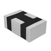
Figure 1. PMOS Transistor
What is PMOS Transistor?
PMOS transistor or P-channel Metal-Oxide Semiconductor, is a type of electronic switch used to control the flow of electricity in a circuit. It works by using holes (which are like missing electrons) to carry current. It has three main parts: the source, the drain, and the gate. The gate decides if electricity can flow from the source to the drain.

Figure 2. PMOS transistor Symbol
The PMOS turns on (lets current flow) when the gate voltage is lower than the source voltage. It turns off (blocks current) when the gate voltage is the same or higher than the source voltage. PMOS transistors are made using n-type material for the base, and p-type material for the source and drain.
PMOS work the opposite way of NMOS transistors. Both are used in CMOS circuits, which are found in devices like phones and computers. PMOS is a bit slower, but it uses less power when it's off, which helps save energy.
PMOS Transistor Structure

Figure 3. Cross-Sectional Structure of a PMOS Transistor
A PMOS transistor is built on n-type substrate, also called the bulk. Into this base, two p-type regions are placed—one acts as the source, and the other as the drain. On top of the area between the source and drain is a thin insulating layer called the gate oxide, and above that is the metal gate.
The gate controls whether current can flow between the source and drain. The metal contacts connect the source and drain to the rest of the circuit. When the gate voltage is low, holes (positive charges) form a path between the source and drain, allowing current to flow. When the gate voltage is high, this path disappears, and the transistor turns off.
Main parts:
• n-type substrate (bulk) – base layer
• p-type source and drain – allow current flow
• Gate oxide – insulation between gate and channel
• Metal gate – controls the switch
• Metal contacts – connect to the outside circuit
This structure allows the PMOS transistor to act like a controlled switch in digital and analog electronics.
Applications of PMOS Transistors
CMOS Circuits - PMOS is used together with NMOS in CMOS chips, which are found in phones, computers, and digital devices.
Works as a Switch - PMOS can turn parts of a circuit on or off, like an electronic switch.
Pull-Up in Digital Circuits - PMOS is used to keep a signal high (logic 1) when required.
Analog Circuits - It helps control current in things like amplifiers and mirrors.
PMOS Transistor Circuit Diagram
The diagram below shows how a NAND gate is built using PMOS and NMOS transistors. A NAND gate is a basic digital logic gate that outputs low (0) only when both inputs are high (1). If at least one input is low (0), the output stays high (1). This is the opposite of how an AND gate works.

Figure 4. CMOS NAND Gate Circuit
In the circuit:
• When A = 0 and B = 0, both PMOS transistors are on, and both NMOS transistors are off. The output is connected to the power supply (VDD) and not to ground, so the output is 1.
• When A = 0 and B = 1, one PMOS is on, and one NMOS is off. The output remains connected to VDD, so it stays 1.
• When A = 1 and B = 0, the other PMOS is on, and the other NMOS is off. The output is still connected to VDD, so it remains 1.
• When A = 1 and B = 1, both PMOS are off, and both NMOS are on. Now, the output is disconnected from VDD and connected to ground, so it becomes 0.
Truth Table
The threshold voltage (Vth) of a PMOS transistor is the gate-to-source voltage (Vgs) at which the transistor starts to turn ON by forming a channel.
In PMOS:
• The source is usually connected to the positive supply voltage (Vdd).
• To turn it ON, the gate voltage must be lower than the source voltage.
• Since the source is at a higher voltage (Vdd), and the gate is lowered, Vgs = Vg - Vs becomes negative, allowing the PMOS to turn ON.
When Vgs becomes more negative than the threshold voltage (which is itself a negative value), the PMOS channel inverts, and current flows from source to drain.
|
A |
B |
PMOS Status |
NMOS Status |
Output |
|
0 |
0 |
Both ON |
Both OFF |
1
(Connected to VDD) |
|
0 |
1 |
One ON |
One OFF |
1 (Still
connected to VDD) |
|
1 |
0 |
One ON |
One OFF |
1 (Still
connected to VDD) |
|
1 |
1 |
Both OFF |
Both ON |
0
(Connected to GND) |
PMOS vs NMOS: What's the Difference?
PMOS and NMOS are two types of MOSFET (Metal-Oxide-Semiconductor Field-Effect Transistor) technologies used in digital and analog circuits. While both control the flow of current using an electric field, they behave differently based on voltage and internal structure. Here's a side-by-side comparison:
|
Feature |
PMOS |
NMOS |
|
Full Name |
P-channel
MOSFET |
N-channel
MOSFET |
|
Major
Carriers |
Holes |
Electrons |
|
Current
Flow |
From
source to drain when Vgs < Vth(negative) |
From
source to drain when Vgs > Vth (positive) |
|
Turns ON
When |
Gate
voltage is LOW |
Gate
voltage is HIGH |
|
Symbol
Arrow |
Arrow
outward from source |
Arrow
inward to source |
|
Speed |
Slower
(holes move slower) |
Faster
(electrons move faster) |
|
Power
Consumption |
Slightly
higher when ON |
More
efficient in switching |
|
Used in |
Pull-up
networks |
Pull-down
networks |
|
Threshold
Voltage |
Typically
negative |
Typically
positive |
|
Area on
Chip |
Takes more
space |
More
compact |
|
Leakage
Current |
Generally
lower |
Slightly
higher in OFF state |
|
Mobility
of Carriers |
Lower hole
mobility |
Higher
electron mobility |
|
Fabrication
Cost |
Higher due
to larger area |
Lower due
to compact design |
|
Noise
Margin |
Better resistance
to noise |
Slightly
more sensitive to noise |
|
Common Use
in Logic |
Used in
CMOS for PUN (Pull-Up Network) |
Used in
CMOS for PDN (Pull-Down Network) |
|
Power
Supply Behavior |
Connects
to VDD (positive rail) |
Connects
to GND (ground rail) |
|
Drive Strength |
Weaker
drive strength |
Stronger
drive strength |
Conclusion
PMOS transistors are important electronic parts because they save power. They are perfect for devices like phones and tablets. Understanding PMOS helps you build better electronic circuits.
function test. The highest cost-effective products and the best service is our eternal commitment.
Hot Article
- LM358 Dual Operational Amplifier Comprehensive Guide: Pinouts, Circuit Diagrams, Equivalents, Useful Examples
- Are CR2032 and CR2016 Interchangeable?
- Understanding the Differences ESP32 and ESP32-S3 Technical and Performance Analysis
- Choosing the Right Battery: A Guide to AG4, LR626, LR66, 177/376/377, SR626, and SR626SW Equivalents
- BC547 Transistor Basics: Pinout, Application Circuits, Alternative/Complementary Models
- NPN vs. PNP: What's the Difference?
- esp32 vs stm32: which microcontroller is better for you?
- What Is a MOSFET and How It Works?
- Electrical Relay Basic: Working Operation, Types and Uses
- PNP Transistors: Structure, Working Principle and Application
 What Is a Capacitor? Definition, Uses & Formulas in Series and Parallel
2025-05-20
 Exploring MOSFET Transistors: Structure, Function, and Applications
2024-06-27
Frequently Asked Questions [FAQ]
1. Is PMOS better than NMOS?
Not necessarily. PMOS is slower but consumes less power when off. NMOS is faster and smaller, making both useful in different roles.
2. Why does PMOS use holes as carriers?
Because PMOS uses p-type regions for source and drain, holes are the majority carriers that move current.
3. Does PMOS require a negative voltage to turn on?
No external negative voltage is needed; just a gate voltage lower than the source is enough (Vgs must be negative).
4. Are PMOS transistors more power-hungry than NMOS?
PMOS uses more area and is slower, but it consumes less power when off, making it good for standby functions.
5. What is the role of gate oxide in PMOS?
The gate oxide insulates the gate terminal from the channel and allows voltage control without direct current flow.
Hot Part Number
 CX0805MRX7R8BB223
 CGA2B2X8R1H152M050BE
 08055U101KAT4A
 CC0603JRX7R8BB224
- 08055U5R6BAT2A
 06035U5R6CAT2A
 12065C105JAT2A
 GRM1886S1HR90CD01D
 TBJD476K016LSSB0023
 BDW84C
- X1205S8I
- VE-220-IY
- VI-JWB-MZ
- KP236N6165XTMA1
- MCC40-10I08
- T491D336K025ATAUTO7280
- TRSF3243CPWR
- AM5728BABCXEA
- LC75833W-TBM-E
- UCC2892PWR
- CDC337DWR
- T491C475K025AT2478
- TPS2044BD
- STM32L071RBT6TR
- TPS5410MDREP
- TS5A22364DGSR
- ADT7421ARMZ
- AK4340ET
- ATD97SC3202-X1AC
- CS5532ASZ
- CY14E256LA-SZ25X
- HD155141
- LM4880MX
- M60089H-0201Y
- MB89615-150
- S-93C56BD0I-T8T1GE
- VT261WFQR-ADJ
- MIP2K40MSSCF
- IC41C16100S-50K
- LV1605ML-MPB-E
- PSN76025A0
- BQ40Z80RSMT
- VT1622AG
- ANA37326B
- AND0241RM27Q7
- CXD2913AQ
- CY7C1382D-200BZXC
- GD25Q64CFIG
- RGTVX6TS65DGC11