Ultimate Beginner’s Guide to Surface Mount Technology (SMT) in Electronics
2025-07-22
8498
Catalog

Figure 1. Surface Mount Technology
What is Surface Mount Technology SMT?
Surface Mount Technology (SMT) is a method of assembling electronic circuits in which components are mounted directly onto the surface of a printed circuit board (PCB). Unlike traditional Through-Hole Technology, which requires components to be inserted into drilled holes, SMT allows for components to be placed and soldered directly onto the PCB surface.

Figure 2. SMT Component Soldered on PCB
This technology originally developed in the 1960s and gaining widespread adoption by the late 1980s. SMT revolutionized electronic manufacturing by enabling more compact, efficient, and automated assembly. Components used in SMT are specifically designed with flat metal leads or terminations that allow for direct attachment to the PCB using soldering techniques such as reflow soldering.

Figure 3. Surface-Mount Devices (SMDs) on a Printed Circuit Board (PCB)
SMT Key Components
• Surface Mount Devices (SMDs) – Small leadless components soldered directly to the PCB. These components include resistors, capacitors, inductors, diodes (like Zener and Schottky), transistors (BJT and MOSFET), and integrated circuits such as logic chips, op-amps, and microcontrollers.
SMDs come in standard sizes for passive components, including 0402, 0603, 0805, and 1206.
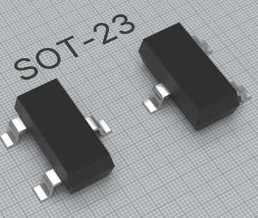
Figure 4. SMT Component Transistor
Diodes and transistors typically use packages like SOD-123, SOT-23, and SOT-223.

Figure 5. Integrated Circuit IC
ICs are available in formats such as SOIC, TSSOP, QFN, COB, and BGA, depending on the complexity and pin count.
• Surface Mount Connectors – Compact connectors mounted on the PCB for device interfacing. Examples include USB, HDMI, RJ45 (Ethernet), audio jacks, board-to-board, and FPC/FFC connectors.
• Surface Mount Power Components – Components for power regulation and switching. Includes voltage regulators, power MOSFETs, DC-DC converters, PMICs, and surface-mount fuses.
• Surface Mount LEDs and Emitters – Light-emitting and light-detecting components. Examples are SMD LEDs (single/RGB), IR LEDs, photodiodes, phototransistors, and optocouplers.
• Surface Mount Sensors – Sensors for measuring physical or environmental conditions. Includes temperature sensors, accelerometers, gyroscopes, magnetometers, pressure sensors, and gas sensors.
• Surface Mount Crystals and Oscillators – Components for generating precise timing signals. Includes quartz crystals, MEMS oscillators, TCXO, and VCXO in small SMT packages.
• Surface Mount Antennas – Wireless communication components mounted on PCBs. Examples include chip antennas, ceramic antennas, patch antennas, and flexible SMT antennas for Wi-Fi, GPS, and Bluetooth.
• Surface Mount Transformers and Filters – Used for signal isolation and noise suppression. Includes SMT transformers, ferrite beads, common mode chokes, and EMI filters.
Surface Mount Technology Assembly Process
Below is a step-by-step overview of how the SMT manufacturing process works.
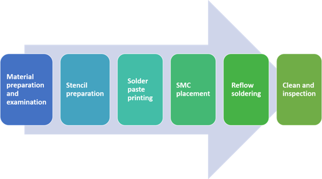
Figure 7. Surface Mount Technology Manufacturing Process
Step 1. Material Preparation and Examination
The SMT process starts with preparing and examining the materials. Printed Circuit Boards (PCBs) and Surface Mount Devices (SMDs) are inspected for quality and compatibility. The PCB features flat, metallic solder pads–coated with tin-lead, silver, or gold–that serve as component attachment points. A metal stencil is also prepared at this stage, designed to match the PCB layout and guide accurate solder paste application.
Step 2. Stencil Preparation
The stencil, typically made of stainless steel, is aligned precisely over the PCB. This template contains openings corresponding to the solder pad locations. Proper stencil setup is important to ensure uniform and accurate deposition of solder paste in the next step.
Step 3. Solder Paste Printing
A solder paste printer spreads paste over the stencil using a squeegee angled between 45°–60°. The paste is a mix of tiny solder particles and flux, which helps clean surfaces and temporarily hold components. The paste passes through the stencil openings and deposits on the PCB’s solder pads. Consistency matter–too much or too little paste can lead to defects like shorts or weak connections.
Step 4. SMC (Surface Mount Component) Placement
Automated pick-and-place machines accurately position SMDs onto the solder-pasted PCB. These high-speed machines use vacuum nozzles or mechanical grippers to place thousands of components per hour with pinpoint accuracy. Any misalignment can result in later functional failures or costly rework.
Step 5. Reflow Soldering
The populated PCB enters a reflow oven, where controlled heating zones gradually raise the temperature to melt the solder paste. This forms solid, electrical, and mechanical bonds between components and the PCB. The oven typically consists of preheat, soak, reflow, and cooling zones. Precise temperature profiles are essential to avoid incomplete solder joints or component damage.
Step 6. Clean and Inspection
Post-reflow, the assembly may undergo cleaning to remove flux residues. The final inspection phase includes Automated Optical Inspection (AOI), X-ray inspection for hidden joints (e.g., BGAs), and electrical tests. Any defects detected are reworked before the boards move to final assembly or packaging.
Types of SMT Surface Mount Technology
This section outlines the three main types of SMT–Type I, Type II, and Type III–and explains when each is most appropriate.
Type I SMT: Standard Surface Mount
Type I SMT uses only surface mount devices (SMDs) and no through-hole components. Components may be placed on one or both sides of the PCB. A single-sided layout is simple and low-cost, ideal for basic electronics like LED boards or small gadgets. A double-sided design increases component density but requires an extra reflow process. Type I is best for compact, low-complexity products that don’t need mechanical reinforcement.
Type II SMT: Mixed Technology on One Side
Type II combines SMDs and through-hole components on the primary side of the PCB, while the secondary side contains only SMDs. This approach balances space efficiency with mechanical strength, using through-hole parts for connectors or heavy components. Reflow soldering is used for SMDs, and wave soldering for through-hole parts. Type II suits industrial systems, power electronics, or mixed-technology consumer devices.
Type III SMT: Split Mixed Technology
Type III also mixes surface mount and through-hole components but places through-hole parts only on the primary side. The secondary side is dedicated to SMDs. This layout supports mechanical stability and better thermal management while allowing dense SMT placement on the reverse side. Like Type II, it requires both reflow and wave soldering. Type III is ideal for designs with top-mounted connectors or structural elements.
SMT Types Comparison
|
Criteria |
Type
I |
Type
II |
Type
III |
|
Component Type |
SMDs only |
SMDs and through-hole on one side |
Through-hole on primary, SMDs on secondary |
|
Complexity |
Low to medium |
Medium to high |
Medium to high |
|
Cost |
Lowest |
Moderate |
Moderate |
|
Mechanical Strength |
Low |
High |
High |
|
Best For |
Simple electronics |
Industrial or mixed-use systems |
Connector-heavy or thermally managed
boards |
SMT Advantages and Disadvantages
|
Category |
Advantages |
Disadvantages |
|
Design & Size |
- Supports compact, lightweight PCB
layouts- Allows higher component density on both sides of the board- Enables
smaller and more portable electronic devices |
- Components are fragile and more prone
to damage- Limited mechanical strength under stress or vibration |
|
Assembly Process |
- Enables fast, automated assembly-
Suitable for high-volume production- Minimizes human error |
- Requires precise soldering and thermal
control- Difficult and time-consuming to repair or rework- High complexity in
the soldering process |
|
Cost & Efficiency |
- Reduces long-term production costs-
Uses smaller and cheaper components- Saves material and board space |
- High upfront investment in SMT
machinery and inspection tools- Not cost-effective for low-volume production |
|
Performance |
- Improved electrical performance due to
shorter signal paths- Suitable for high-speed and high-frequency circuits-
Lower parasitic effects (resistance and inductance) |
- Greater risk of thermal issues due to
compact design- Limited heat dissipation without additional cooling design |
|
Flexibility |
- Compatible with double-sided PCB
assembly- Can be used with through-hole components in hybrid designs |
- Component miniaturization increases
difficulty in manual inspection- Requires continuous updates to keep up with
new SMT technology |
|
Quality Control |
- Supports automated inspection systems
like AOI and X-ray- Delivers consistent quality in large batches |
- Visual inspection is ineffective for
small and densely packed boards- Advanced inspection adds to overall
equipment cost |
|
Workforce & Skills |
- Reduces manual labor through
automation- Simplifies repetitive assembly tasks |
- Demands specialized training and technical
expertise- Higher learning curve for operators and engineers |
Applications of Surface Mount Technology
• Consumer Electronics – SMT is used in smartphones, laptops, tablets, and gaming devices for compact, high-performance designs.
• Automotive Electronics – Powers systems like ECUs, infotainment, lighting, and ADAS with durable and space-saving components.
• Industrial Equipment – SMT supports PLCs, motor drives, and automation systems with reliable, compact circuit designs.
• Medical Devices – Enables precise, portable devices such as imaging systems, monitors, and diagnostic tools.
• Telecommunications – SMT technology drives high-speed network gear like routers, modems, and satellite communication systems.
• Aerospace and Defense – Used in avionics, radar, and military systems requiring compact, rugged performance.
• Smart Home and Appliances – SMT integrates control systems in smart thermostats, refrigerators, washers, and other connected appliances.
Surface Mount Technology Challenges
As devices grow smaller and more powerful, SMT introduces a range of engineering challenges. These challenges affect thermal performance, cost, and reliability. Addressing them early in the design and production process matter for success.
Component Availability and Supply Chain Risks
SMT production often relies on specific components with limited substitutes. Global supply chain issues, such as material shortages or geopolitical disruptions, can delay projects and force last-minute design changes. Engineers may need to qualify alternate components or redesign boards to maintain production schedules.
Miniaturization and Layout Constraints
As devices shrink, fitting more functionality into smaller boards becomes increasingly difficult. High component density can lead to complex routing, reduced clearances, and signal integrity challenges. Engineers must balance performance, thermal behavior, and manufacturability within tight space constraints. Smaller parts are also more difficult to inspect, handle, and rework, increasing the risk of error during production.
Inspection and Testing Complexity
Traditional visual inspection is no longer enough for high-density assemblies, especially those with hidden solder joints like BGAs. Manufacturers now rely on X-ray inspection, in-circuit testing, and automated systems to ensure quality. These tools add cost and complexity but are critical for identifying defects that would otherwise go undetected.
Component Orientation and Polarity Errors
With miniature parts, it is easier to misplace components or install them with the wrong polarity. Manual assembly or rework increases the chance of error, which can lead to board failures that are difficult to trace. Ensuring consistent orientation markings, proper documentation, and automated validation helps prevent these mistakes.
Moisture Sensitivity and Storage Requirements
Some SMT components are sensitive to moisture. If exposed to humidity, they can absorb water and crack during reflow, a condition known as “popcorning.” Proper storage in controlled environments and baking procedures before assembly are necessary to avoid moisture-related failures.
EMI and EMC Challenges
As boards become more compact and carry faster signals, electromagnetic interference becomes a greater concern. Poor layout or grounding can result in failed compliance tests or erratic system behavior. You must carefully design shielding, trace routing, and return paths to meet electromagnetic compatibility requirements.
Surface Mount Technology vs. Through Hole Technology

Figure 8. SMT vs. THT
|
Feature |
Through-Hole
Technology |
Surface
Mount Technology |
|
Component Size |
Utilizes bulkier components ideal for
rugged applications |
Employs miniature components suited for
compact designs |
|
Manufacturing Speed |
Slower production pace due to manual
handling and drilling |
High-speed automated assembly enhances
production output |
|
Assembly Process |
Involves manual insertion of leads into
pre-drilled holes |
Automated placement directly onto PCB
surface pads |
|
Board Real Estate |
Occupies more space due to hole and lead
structure |
Conserves PCB space, allowing tighter
and more efficient layouts |
|
Mechanical Durability |
Offers superior mechanical bonding,
ideal for connectors and stress points |
Less durable under mechanical strain or
vibration |
|
Thermal Management |
Leads provide additional thermal
dissipation |
May require thermal vias or heat sinks
for better heat dispersion |
|
Soldering Techniques |
Supports both manual and machine
soldering |
Primarily relies on automated soldering
processes |
|
Power Application |
Designed to handle higher current and
voltage loads |
More effective in low- to moderate-power
circuitry |
|
Circuit Density |
Limits component density due to spacing
and drilling needs |
Enables high component density for
complex, multilayer boards |
|
Prototyping Compatibility |
Preferred for prototyping and testing
environments |
Less suited for hand prototyping due to
small scale |
|
Rework Simplicity |
Easier to desolder and replace
components |
Repairs can be intricate, especially on
dense boards |
|
Surface Finish |
Often finished with non-planar HASL
coatings |
Features flat finishes like ENIG, OSP,
or Immersion Silver |
|
Design Adaptability |
Less flexible in compact designs due to
size constraints |
Highly adaptable to intricate and
space-saving PCB layouts |
|
Lead Configuration |
Requires holes for through-lead mounting |
Mounted via flat pads with no holes |
|
Stencil Usage |
Typically not needed during assembly |
Requires solder paste stencil unless
it's a simple design |
|
Two-Sided Mounting |
Less common; mostly single-sided
configurations |
Regularly supports double-sided
component placement |
|
Test Accessibility |
Test points are larger and easier to
probe manually |
May include both SMT and through-hole
test access points |
|
Environmental Tolerance |
Better resilience in harsh or extreme
environments |
More susceptible to environmental and
mechanical stress |
|
Fiducial Pad Need |
Does not require fiducial marks for
assembly |
Needs fiducial pads for automated
pick-and-place machines |
|
Material Heat Tolerance |
Works with standard laminate
temperatures (~130°C Tg) |
Often uses high-temp laminates (~170°C
Tg) |
|
Availability of Parts |
Becoming less common as SMT dominates
the market |
Widely supported by modern component
manufacturers |
|
Cost Efficiency |
Higher cost due to extra materials and
manual work |
More cost-effective for mass production |
|
Inspection Method |
Can be visually inspected with basic
tools |
Needs AOI or X-ray inspection for
accuracy |
|
Twist and Warp Resistance |
Tolerates minor warping during assembly |
Sensitive to warping; flatness is
critical |
|
Hole via Integration |
Cannot incorporate vias under components |
Supports via-in-pad design for signal integrity |
Future of Surface-Mount Technology (SMT)
Surface-Mount Technology (SMT) is evolving to meet the growing demand for smaller, faster, and more efficient electronic devices. This progress is driven by the integration of advanced materials, smarter production methods, and intelligent automation.
Flexible substrates and conductive inks are enabling lighter, more durable, and energy-efficient designs, especially in wearables and flexible electronics. At the same time, 3D printing is speeding up PCB production by allowing precise, multi-layered board fabrication, which shortens development cycles.
Sustainability is also a growing focus. Manufacturers are adopting lead-free solder and reducing waste, with SMT supporting more eco-friendly practices. Meanwhile, artificial intelligence is improving design and manufacturing by optimizing layouts, detecting defects, and increasing overall efficiency.
These advancements are keeping SMT at the core of modern electronics, driving innovation while meeting the industry’s need for performance, and sustainability.
function test. The highest cost-effective products and the best service is our eternal commitment.
Hot Article
- LM358 Dual Operational Amplifier Comprehensive Guide: Pinouts, Circuit Diagrams, Equivalents, Useful Examples
- Are CR2032 and CR2016 Interchangeable?
- Understanding the Differences ESP32 and ESP32-S3 Technical and Performance Analysis
- BC547 Transistor Basics: Pinout, Application Circuits, Alternative/Complementary Models
- Choosing the Right Battery: A Guide to AG4, LR626, LR66, 177/376/377, SR626, and SR626SW Equivalents
- NPN vs. PNP: What's the Difference?
- esp32 vs stm32: which microcontroller is better for you?
- What Is a MOSFET and How It Works?
- Electrical Relay Basic: Working Operation, Types and Uses
- PNP Transistors: Structure, Working Principle and Application
 What is LCR Meter? Definition, Types, Circuit Techniques
2025-07-24
 How a Capacitor Works in a DC Circuit?
2025-09-02
Frequently Asked Questions [FAQ]
1. What are the component packages in SMT?
Common SMT packages include SOIC, QFP, BGA, tantalum capacitor packages, and ceramic packages.
2. What are the sizes of SMD Components?
Common sizes include 0201, 0402 (0.04" × 0.02"), 0603, 0805, and 1206.
3. What are the dimensions of an SMD transistor package?
The SOT-23 package typically measures about 3 mm × 1.75 mm × 1.3 mm.
4. What are common SMT soldering defects and how do you prevent them?
Common SMT defects include solder bridging, tombstoning, and cold joints. Prevent them with correct stencil design, solder paste volume, and precise thermal profiles.
5. What’s the difference between reflow and wave soldering in SMT?
Reflow soldering is used for SMT components by melting solder paste in an oven, while wave soldering is used for through-hole parts via a solder wave bath.
6. Can SMT components be manually soldered?
Yes, but it's challenging. Manual SMT soldering is possible with precision tools, magnification, and controlled heating–mostly for prototypes or rework.
7. How does stencil design affect SMT soldering quality?
Stencil thickness, aperture size, and alignment directly influence solder volume, which affects joint strength, bridging risk, and component reliability.
8. How do you choose between SMT and THT for your PCB design?
Use SMT for high-density, compact, and automated builds; choose THT for mechanical strength, high-power components, or prototyping simplicity.
Hot Part Number
 CGA9N3X7S2A106K230KB
 C3216X7S0G476M160AB
 CL05B562KA5NNNC
 CGA3E3X8R2A333M080AD
 1206PC473KAT2A
- CL10C151GB8NNWC
 GCM1555C1H391JA16D
 GRM1885C2A8R0DA01J
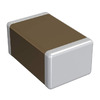 GQM2195C1H470GB01D
 GRM0336R1E1R2CD01D
- T510E108M004AS4115
- BZT52C5V1T-7
- 843252AGLFT
- RTC-72421B
- LAN9514-JZX-TR
- XRT86VX38IB256-F
- VI-JT3-EW
- EP1S25F1020C5
- S912B32E4VFUE8R
- V48C12C150B
- V300A48M500BL
- 6MBI35S-140-50
- NCV2903DMR2G
- CAT3200ZI-GT3
- ADG721BRMZ-REEL
- T491D106M035AT7128
- F6KA2G605A4LA-Z
- AD9226ARSZRL
- ADS8341EB
- LC898212XD-SH
- TPS2541RTET
- LP2953IM-3.3
- ADF4106BRUZRL
- ATAR862N-087-TNQ38
- BCM5751MKFBG
- BQ20881DBTR
- EL2120CS
- K4B4G1646E-BCK0
- M5M5V108DKV-70HI
- MC14051BCP
- MPC993FA
- PI3HDMI2410-AFFE
- XCS20XL5TQ144C
- APA2621RI-TRG
- DS24B33S+T&R
- IDT71V321L25TFI
- RTL8366S-VS-GR
- SKKT215/16E
- EXO-3C16MHz