Explore the Principles, Symbols, and Applications of Depletion-Mode MOSFETs
2024-06-05
17655
Catalog

Figure 1: MOSFET
What Is a Depletion-Type MOSFET?
A depletion-type MOSFET is a metal oxide semiconductor field effect transistor that can remain in the "on" state without an external gate voltage. In actual use, the gate of this device usually does not require a positive voltage to allow current to flow, so it is called a "normally on device." When no gate voltage is applied, the channel between the drain and the source is in an open state, allowing free current to flow.

Figure 2: Depletion Mode MOSFET Structure
Applying a negative voltage to the gate increases the resistance of the gate-source channel. This is because the negative voltage attracts positive charges to the gate, which pushes away the free electrons in the channel. As a result, the electron flow path becomes narrower and the channel resistance increases. As the gate voltage becomes more negative, the current between the source and drain decreases until it stops completely.
In circuit design, the "normally on" nature of the depletion-mode MOSFET is very useful. For example, protection or startup circuits that need to quickly cut off the current can provide an instant current path without waiting for an external control signal. In addition, because this MOSFET remains on in the absence of gate voltage, it is particularly useful in low-power and high-reliability environments, such as remote sensors or emergency shutdown systems.
Depletion MOSFET Symbol
There are two main variations of the depletion-mode MOSFET symbol: P-channel and N-channel. The direction of the arrow in the symbol distinguishes the channel type. If the arrow points inward, it indicates an N-channel MOSFET. If it points outward, it indicates a P-channel MOSFET. This design makes reading and drawing circuit diagrams simpler.

Figure 3: N-Channel Symbol

Figure 4: P-Channel Symbol
In circuit design, the standard depletion-mode MOSFET symbol includes three main parts: source, drain, and gate. The source and drain are connected by a line, and the gate branches off this line. The arrow points from the gate to the source or from the source to the source, which helps determine the channel type.
Understanding and recognizing these symbols can help prevent incorrect connections that could cause circuit failure or equipment damage when assembling complex circuits with multiple MOSFET types. These symbols allow designers to quickly identify component properties, ensuring correct placement and connection.
In addition, these symbols help identify components during testing and maintenance. When repair technicians diagnose circuit problems, they can use these symbols to quickly locate the problem. For example, they can check if the gate voltage is incorrectly applied to a specific MOSFET type. Accurate symbol representation simplifies failure analysis and increases the efficiency of the troubleshooting process.
Working Principle of Depletion MOSFET
A depletion-mode MOSFET is naturally conducting in the absence of an external gate voltage (V_GS = 0V). In this state, a conducting channel formed by free carriers (usually electrons) exists between the source and drain, allowing current to flow freely. This natural conductive property makes depletion-mode MOSFETs the default switch in many circuits.

Figure 5: Depletion Mode MOSFET Circuit Diagram
When a negative voltage is applied to the gate of an N-channel depletion-mode MOSFET, the operation changes subtly. The negative voltage repels electrons in the gate region toward the source, reducing the free carrier density in the channel near the gate. As the negative voltage increases, the free carriers in the channel decrease until the channel is completely "depleted," shutting off the flow of current.
Conversely, applying a positive voltage to the gate attracts more electrons into the channel, increasing the density of free carriers. This enhances the conductivity of the channel, increasing the current flow between the source and drain. This process allows the MOSFET channel to be precisely controlled by adjusting the polarity and magnitude of the gate voltage, thereby regulating the current.
In power management circuits, depletion-mode MOSFETs are used to fine-tune power supply output or as variable resistors in analog signal processing. In these applications, understanding the MOSFET's response to gate voltage facilitates precise circuit control and optimization. Operators need to be familiar with the MOSFET's behavior at different gate voltages to achieve the desired performance in the circuit.
Drain Characteristics of P-Channel Depletion MOSFET
The drain characteristics of a P-channel depletion-mode MOSFET are determined by the drain-source voltage (V_DS) and the gate-source voltage (V_GS). When V_DS is negative, it means that the voltage is applied from source to drain, and the setting is opposite to that of an N-channel MOSFET. If V_GS is positive, the drain current (I_D) decreases as V_GS increases. This is because positive voltage reduces the number of holes (carriers in a P-channel MOSFET) in the channel, thereby weakening its conductivity.
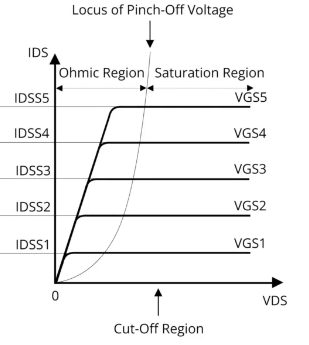
Figure 6: Drain Characteristics of P-Channel Depletion MOSFET
When V_GS increases to a certain point, the MOSFET enters a pinch-off state, pushing all holes out of the channel, and causing the drain current I_D to drop to zero, enabling precise current control. Conversely, applying a negative voltage to V_GS increases the number of holes in the channel, causing the drain current I_D to rise above the drain saturation current (IDSS).
Understanding these characteristics facilitates circuit design and optimization. Engineers must precisely control V_GS to exploit these characteristics of the P-channel depletion MOSFET to achieve the desired low or high current output. For example, in load regulation or current limiting applications, accurately regulating V_GS enables fine current control, ensuring stable operation and long-term reliability of the circuit.
Transfer Characteristics of P-Channel Depletion MOSFET
The transfer characteristics of a P-Channel depletion-mode MOSFET are very different from those of an N-Channel depletion-mode MOSFET. In actual operation, these characteristics show how the gate-source voltage (V_GS) regulates the drain-source current (I_D). When V_GS is positive, I_D gradually increases from zero. As V_GS continues to rise, the current reaches IDSS, the maximum saturation current, reflecting the gradual increase in channel conductance.
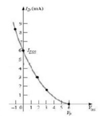
Figure 7: Transfer Characteristics of P-Channel Depletion MOSFET
When V_GS becomes negative, the P-Channel MOSFET allows the current to continue to increase. This unique characteristic of the depletion-mode MOSFET means that increasing the negative gate-source voltage reduces the hole repulsion within the channel, further enhancing the current flow. This behavior is opposite to that of an N-Channel MOSFET, where increasing negative V_GS reduces the current.
Designers need to ensure that the P-Channel MOSFET provides enough current at negative V_GS in applications such as power management or analog signal conditioning so that it can be used for reverse voltage operation.
To maximize circuit performance and efficiency, engineers analyze these transfer characteristics through detailed lab testing. This includes plotting ID-VGS curves and accurately determining the I_D values at different V_GS. With this data, the performance of the MOSFET in the actual circuit can be accurately simulated and predicted, allowing more informed design decisions to be made.
Drain Characteristics of N-Channel Depletion-Mode MOSFET
Understanding the drain characteristics of an N-channel depletion-mode MOSFET enables effective use. As the drain-source voltage (V_DS) rises, the drain current (I_D) of this MOSFET increases until it reaches a point called the saturation current (IDSS), typically when the gate-source voltage (V_GS) is 0V.
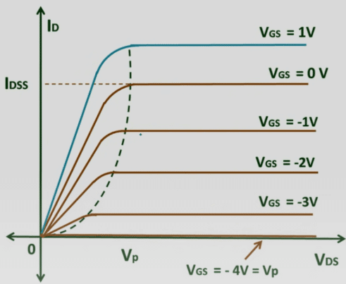
Figure 8: Drain Characteristics of N-Channel Depletion-Mode MOSFET
As V_DS increases, the drain current initially rises, reflecting the freer movement of electrons in the channel. However, once the current reaches saturation, the current remains constant even if V_DS increases further because the electron velocity in the channel is close to the maximum value.
When a negative voltage is applied to the gate, it repels the electrons in the channel to the P-type substrate, causing them to recombine with holes. This electron-hole recombination reduces the number of free electrons, thus reducing the current. As negative V_GS increases, the recombination rate accelerates, further depleting the channel of electrons until the current reaches zero at the pinch-off voltage.
Conversely, applying a positive V_GS attracts more electrons into the N channel, increasing the electron density and channel conductivity, thereby raising the current I_D above IDSS. This allows precise control of the current by adjusting V_GS, suitable for applications that require fine current regulation.
During circuit design or debugging, engineers closely monitor these characteristics. They use laboratory equipment to observe the relationship between V_DS and I_D to ensure that the MOSFET operates within a safe and optimal range. Understanding these drain characteristics not only enhances circuit reliability but also enables effective current control, optimizing the performance of the entire system.
Transfer Characteristics of N-Channel Depletion MOSFET
The transfer characteristics of an N-Channel depletion-mode MOSFET describe how the drain current (I_D) varies with the gate-source voltage (V_GS) at a fixed drain-source voltage (V_DS). This relationship directly affects circuit behavior and performance.

Figure 9: Transfer Characteristics of N-Channel Depletion MOSFET
When V_GS is positive, I_D increases as V_GS increases. This is because positive V_GS attracts more electrons into the channel, which reduces resistance and increases current. This occurs in the "enhancement region," where more electrons make the channel more conductive.
Conversely, when V_GS is negative, the MOSFET enters the "depletion region." Here, negative V_GS repels electrons from the channel, which increases resistance and reduces current. By adjusting the negative V_GS, engineers can precisely control the reduction in current until it is completely cut off.
The relationship between drain current and gate-source voltage can be described by the following equation: 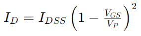 .This shows that I_D depends on the ratio between V_GS and the pinch-off voltage (V_P), which is the voltage at which the MOSFET is fully turned off. This equation helps engineers predict the current behavior at different V_GS values, which can optimize MOSFET applications.
Engineers use this relationship to design and troubleshoot circuits. For example, when designing amplifiers or switching circuits, they can use this equation to adjust V_GS to achieve the desired I_D. It also forms the basis for simulating MOSFET behavior in circuit simulation software, allowing accurate predictions and adjustments in real-world applications.
Working Principle of P-Channel Depletion-Mode MOSFET
P-channel depletion-mode MOSFET consists of a P-type channel formed by a P-type semiconductor material, with an N-type semiconductor substrate. The main carriers in this device are holes, which flow from the source to the drain through the P-type channel. Due to the high doping, the hole concentration in the channel is high, making it highly conductive.
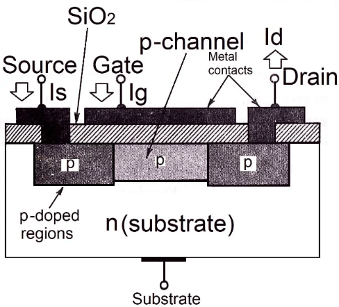
Figure 10: Structure of N-channel depletion-mode MOSFET
When there is no gate voltage (V_GS = 0V), the MOSFET is usually in the "on" state, allowing a large drain current (I_D) to flow. This is because the P-type channel is naturally full of holes, and current can flow easily without additional voltage.
When a positive voltage is applied to the gate, it attracts electrons to the channel area, where they combine with holes to form a depletion region. The production of fixed negative impurity ions reduces the number of holes in the channel, which reduces its conductivity and thus reduces the drain current. By precisely controlling the gate voltage, the degree of channel depletion and the size of the drain current can be fine-tuned.
To completely turn off a P-channel depletion MOSFET, two methods can be used: remove the positive voltage between the source and drain (cut off the drain bias) or apply a negative gate voltage. Applying a negative gate voltage increases the depletion region, further encouraging electrons to combine with holes. This process significantly reduces the number of holes in the channel, causing the current to taper off until it stops completely, effectively turning the transistor off.
Working Principle of N-Channel Depletion-Mode MOSFET
The N-Channel Depletion-Mode MOSFET is a field effect transistor with an N-type semiconductor channel connecting the source and drain, while the substrate is a P-type semiconductor. In this device, electrons are the main carriers that carry current through the N-type channel between the source and drain.
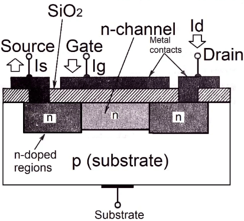
Figure 11: Structure of N-channel depletion-mode MOSFET
This MOSFET does not require an external gate voltage to turn on, which is a key difference from the enhancement-mode MOSFET. When a voltage is applied between the source and drain, current naturally flows through the N-type channel, allowing the transistor to conduct without a gate voltage.
In actual operation, applying a negative gate voltage (V_GS < 0) pushes electrons to the dielectric layer below the N region. This reduces the number of electrons in the channel, forming a depletion region. The formation of this depletion layer reduces the conductivity of the channel, thereby reducing the drain current (I_D). This process enables fine control of current flow, especially in applications that require precise current regulation.
As the negative gate voltage increases, the MOSFET enters pinch-off mode, causing the drain current to further decrease until it stops. Depletion of electrons in the N region becomes the key mechanism for controlling drain current. The combination of drain voltage (V_DS > 0) and negative gate voltage (V_GS < 0) creates a depletion layer near the drain that is wider than the source, which enhances the flexibility and precision of current control.
The operating characteristics of the N-channel depletion-mode MOSFET make it very useful in applications that require fine current control, such as power management, signal modulation, and sensing. Electronic engineers who understand and operate this MOSFET can more effectively design and optimize circuits to ensure efficient operation and long-term stability of the device.
Application of Depletion-Type MOSFET
Depth-mode MOSFETs are widely used in various circuits because they can be turned on without an external gate voltage. Their applications range from basic conduction paths to complex circuit designs and functions.
Constant current source and linear regulator: Depletion-mode MOSFET acts as a pass transistor to provide a stable current or voltage. For example, in a constant current source, the MOSFET ensures a consistent current output regardless of load changes. In a linear regulator, the channel resistance is adjusted by precisely controlling the gate voltage to stabilize the output voltage. Engineers must have a deep understanding of voltage-current relationships and the skills to precisely control these operations.
Startup Auxiliary Power Circuits: Depletion-mode MOSFETs are used in startup circuits to provide the necessary power path when the circuit is initialized. Since they are devices that are turned on by default, they can be powered immediately without complex control signals, ensuring fast startup.
Flyback Circuits in PWM ICs: In pulse-width modulation (PWM) integrated circuits, depletion-mode MOSFETs are used in flyback circuits commonly found in power supplies to achieve efficient power conversion. These MOSFETs are used as switching elements to control high-frequency power transfer, which requires precise timing and voltage control.
Telecom Switches and Solid-State Relays: In telecom and power wiring applications, depletion-mode MOSFETs provide reliable switching functions. Their high reliability and fast response can effectively control a large number of telecom signals or power wiring.
Voltage Sweep and Current Monitoring Circuits: Depletion-mode MOSFETs are used to accurately measure and control voltage and current changes. This enables detailed system monitoring and adjustments, allowing engineers to fine-tune the system for optimal performance.
LED Array Driving Circuits: When driving LED arrays, depletion-mode MOSFETs regulate the current through the LEDs, ensuring proper brightness and color temperature control. This involves complex current control strategies and effective thermal management.
Conclusion
Depth mode MOSFET plays an important role in modern electronic circuit design due to its normally open characteristics and excellent current control ability. Whether in the constant current source, linear regulator circuit, or load resistor in a digital logic circuit, depletion mode MOSFET has shown its unique advantages. By deeply understanding the drain characteristics and transfer characteristics of P-channel and N-channel depletion mode MOSFET, engineers can better design and optimize circuits to meet various application requirements. In addition, the wide application of depletion mode MOSFET in startup auxiliary power supply circuits, flyback circuits in PWM IC, and voltage scanning and current monitoring circuits further proves its importance in electronic systems. Mastering this knowledge will help develop more efficient and reliable electronic products.
Frequently Asked Questions [FAQ]
1. What is the difference between MOSFET and depletion MOSFET?
A MOSFET (Metal-Oxide-Semiconductor Field-Effect Transistor) is a transistor used to amplify and switch electronic signals. It is available in two main types: enhancement and depletion.
Enhancement-mode MOSFET: This type of MOSFET is off when no voltage is applied. To turn it on, a positive (N-channel) or negative (P-channel) voltage needs to be applied between the gate and the source.
Depletion-mode MOSFET: Unlike the enhancement-mode, the depletion-mode MOSFET is naturally on when no voltage is applied. By applying a voltage opposite to the enhancement mode, its ability to conduct electricity can be reduced until it is completely off.
2. How do you increase the depletion region?
Increasing the depletion region in a MOSFET can be achieved by following these steps:
Applying a reverse bias: In a depletion-mode MOSFET, increasing the reverse bias between the gate and source can increase the depletion region. This causes electrons to be pushed away from the depletion region, thereby increasing the width of the depletion region.
Material selection: Choosing a semiconductor material with a higher doping concentration can also affect the width of the depletion region. A high doping concentration generally means a narrower depletion region.
3. Why is the depletion region neutral?
The depletion region is called neutral because the sum of positive and negative charges is equal in this region. Although the number of free carriers (such as electrons and holes) in the depletion region is reduced, the ionized dopant atoms are chemically stable and their positive and negative charges are balanced, so they are electrically neutral overall.
4. Which type of MOSFET is better and why?
Choosing which type of MOSFET is better depends on the application requirements:
Enhancement-type MOSFETs are more suitable for switching applications because they remain off when there is no input voltage, which helps save energy and reduce power consumption.
Depletion-type MOSFETs are suitable for situations where default conduction is required.
Therefore, there is no absolute "better", but it should be selected based on the specific circuit design and functional requirements.
5. What are the disadvantages of MOSFET?
The main disadvantages of MOSFET include:
High sensitivity: MOSFET is very sensitive to static electricity and can be easily damaged by static electricity.
Thermal conductivity issues: When the current increases, MOSFET can generate a lot of heat, and additional heat dissipation measures may be required.
Gate leakage: In some cases, the gate may have a small leakage, which affects the performance of the MOSFET.
function test. The highest cost-effective products and the best service is our eternal commitment.
Hot Article
- LM358 Dual Operational Amplifier Comprehensive Guide: Pinouts, Circuit Diagrams, Equivalents, Useful Examples
- Are CR2032 and CR2016 Interchangeable?
- Understanding the Differences ESP32 and ESP32-S3 Technical and Performance Analysis
- Choosing the Right Battery: A Guide to AG4, LR626, LR66, 177/376/377, SR626, and SR626SW Equivalents
- BC547 Transistor Basics: Pinout, Application Circuits, Alternative/Complementary Models
- NPN vs. PNP: What's the Difference?
- esp32 vs stm32: which microcontroller is better for you?
- What Is a MOSFET and How It Works?
- Electrical Relay Basic: Working Operation, Types and Uses
- PNP Transistors: Structure, Working Principle and Application
 What is a Knock Sensor? How it works, malfunction symptoms
2024-06-05
 Understanding Enhancement-mode MOSFETs: Symbol, Types, and Advantages
2024-06-04
Hot Part Number
 C0603C0G1E9R1C
 C1005CH1H271J050BA
 GRM188R71E392KA01D
 CGJ2B2X7R1H472K050BA
 06031U390GAT2A
 C2012X7R1E155M125AC
 12065C102JAT2A
 12102U131JAT2A
 GQM1555C2D200FB01D
 C3216JB1A156M160AC
- MCP6549-E/ST
- SST39VF3201-70-4I-EKE
- BD7905BFS-E2
- MAX6971AUG+T
- ICL3221EIVZ-T
- VI-2T3-EY
- SST12CP11-QVCE
- RT0402BRE0747R5L
- 2MBI600N-060
- BSM150GB120DN1
- V375A5C400AN
- FDMS86163P
- LTC4366HTS8-2#TRMPBF
- ADS8339IDGSR
- BLUENRG-MSCSP
- TMS320F28375SPZPT
- FS32K144HRT0MLLT
- T491D106M035AT7450
- TPS61200DRCT
- T491X687K006ZTZV13
- LTC2305HMS#TRPBF
- LF444CM
- ADSP2186KST-133
- BDP953E6327
- HS75438DTR
- LFX125B-03F256C
- LMC6035ITLX
- NH82801IO
- SM5852CS
- SP3249ECA-1
- TC74LCX126FT
- GT24C02-2SLI-TR
- STC10F08XE35I-LQFP44
- ALC5684-CG
- M30262F8GP#U3
- SPHE1510A-8BR-HI08N
- ICSU2A877AHLF
- MAX1181ECM+
- BTS5200-1ENA