N-Channel Enhancement-mode MOSFETs in Power Electronics
2025-05-13
29640
Catalog
What is an N-Channel MOSFET?

Figure 1: N-Channel MOSFET Diagram
An N-Channel MOSFET (Metal-Oxide-Semiconductor Field-Effect Transistor) is an electronic switch that controls how current flows through a circuit. It has three terminals: Gate, Drain, and Source, built on an N-type pathway inside P-type silicon. A thin oxide layer insulates the Gate from the rest of the device, so almost no current flows into the Gate itself.
With the Gate at the same (or lower) voltage than the Source, the MOSFET is off and blocks current between the Drain and Source. When you raise the Gate a few volts above the Source, an electric field draws a conductive channel between Drain and Source, turning the device on so electrons can flow from the Drain to the Source.
What is N-Channel Enhancement-mode MOSFET?
An N-channel enhancement-mode MOSFET is like a tiny switch that controls electricity. Most of the time, the switch is off, so no electricity flows through it. But when you add a positive voltage to the Gate, it turns on and lets electricity flow from the Drain to the Source. Since it only turns on when the Gate gets that extra voltage, it's called enhancement-mode. This type of MOSFET improves turn-on and off fast, handles more power than similar switches, and doesn't waste much energy.

Figure 2: N-Channel Enhancement-mode MOSFET Symbol
Working Principle of N-Channel Enhancement-mode MOSFET
Starts (No Channel)
Inside the MOSFET is a slab of p-type silicon with two n-type regions, Drain and Source. With the Gate at the same voltage as the Source, there is no n-type pathway connecting the Drain to the Source, so current can't flow.
Positive Gate Voltage "Enhances" a Channel
Raising the Gate above the Source by at least the threshold voltage (VTH) creates a strong electric field. This field pulls free electrons to the surface, inverting that thin slice of p-silicon into n-type material and forming a conductive channel.
Current Flows from Drain to Source
With the channel in place, applying a positive Drain-to-Source voltage lets electrons travel through it. The higher the Gate-to-Source voltage (VGS), the wider (and lower-resistance) the channel becomes, so more current (ID) can flow.
Two Fields of Operation
• Linear (Ohmic) Region: When the Drain-to-Source voltage (VDS) is small, the MOSFET behaves like a variable resistor; ID rises roughly linearly with VDS.
• Saturation Region: When VDS approaches VGS-VTH, the channel pinches off near the Drain, and ID levels off; the device now acts like a current source set by VGS.
Advantages of Using the Enhancement-mode
• It needs almost no gate current, so it saves power.
• It switches on and off very fast, making it ideal for high-speed circuits.
• Its low on-resistance cuts heat and boosts efficiency.
• It can handle more current than a similar-sized P-channel MOSFET.
• It works with logic-level gate voltages, so a microcontroller can drive it directly.
• It is compact, affordable, and easy to find for most designs.
Device Structure of N-Channel Enhancement-mode MOSFET
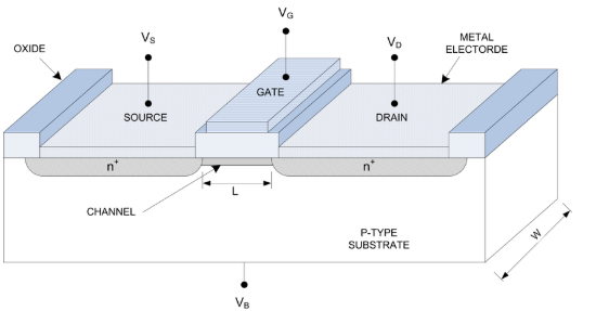
Figure 3: Device Structure of N-Channel Enhancement-mode MOSFET
This diagram shows the internal structure of an N-channel enhancement-mode MOSFET. It's built on a p-type substrate, which is the base material. On top of that, there are two n+ regions called the source and drain, which are the terminals where current enters and exits the device. The gate is placed between them and separated from the substrate by a thin oxide layer. This oxide acts as an insulator, so no current flows into the gate.
When the gate (VG) gets a positive voltage, it attracts electrons under the gate area, forming a channel between the source and drain. This allows current to flow from the drain (VD) to the source (VS). If there's no voltage at the gate, the channel doesn't form, and the MOSFET stays off. The VB label at the bottom shows the voltage applied to the body or substrate.
Applications of N-Channel Enhancement-mode MOSFET
Power Switching
Used to turn devices on and off in power circuits like DC-DC converters, power supplies, and battery protection systems.
Motor Control
Commonly found in H-bridges and PWM circuits for driving DC motors and stepper motors.
Load Drivers
Best for driving high-current loads such as lamps, heaters, and relays.
Amplifiers
Used in analog circuits to amplify small signals in audio, RF, and sensor systems.
Inverter Circuits
The main component in building single-phase or three-phase inverters for solar panels or UPS systems.
Digital Logic Circuits
Used as switches in logic-level circuits and microcontroller GPIO interfaces.
LED Dimming and Control
Used with PWM to control LED brightness in lighting applications.
Battery Management Systems (BMS)
Helps in switching and protecting battery cells in charging and discharging cycles.
Differences Between N-Channel Enhancement-mode and Depletion Mode
|
Feature |
N-Channel Enhancement-mode |
N-Channel Depletion-mode |
|
Default State (No Gate Voltage) |
OFF
(no current flows) |
ON
(current flows) |
|
Turns ON When |
Gate
voltage is positive (VGSthreshold) |
Gate
voltage is zero or positive |
|
Control Behavior |
Needs
a positive voltage to conduct |
Can
be turned off by applying a negative voltage |
|
Symbol (Channel line) |
Broken
line between the drain and source |
Solid
line between the drain and source |
|
Use Case |
Common
in switching and power applications |
Used
in analog and special control applications |
|
Availability |
Widely
available and commonly used |
Less
common, typically used in niche circuits |
|
Power Efficiency |
High
efficiency in switching |
Less
efficient due to default conduction |
N-Channel vs. P-channel Enhancement-mode MOSFET
|
Similarities |
|
|
Feature |
N-Channel
& P-Channel Enhancement-mode MOSFETs |
|
Type |
Both
are enhancement-mode MOSFETs |
|
Control Method |
Both
require a voltage applied to the gate to turn on. |
|
Structure |
Both
have three terminals: Gate, Drain, Source |
|
Application Areas |
Used
in switching, amplification, and power control circuits |
|
High Input Impedance |
The
gate draws very little current. |
|
Fast Switching |
Suitable
for high-speed digital and power applications |
|
Differences |
||
|
Feature |
N-Channel
MOSFET |
P-Channel
MOSFET |
|
Default Conduction Direction |
Current
flows from the Drain to the Source |
Current
flows from Source to Drain |
|
Gate Drive Requirement |
Turns
on when Gate is positive relative to Source |
Turns
on when the Gate is negative relative to Source |
|
Mobility of Carriers |
Uses
electrons (higher mobility) |
Uses
holes (lower mobility) |
|
Switching Speed |
Faster |
Slower |
|
RDS(on) |
Lower |
Higher |
|
Used in Switching Side |
Low-side
switching |
High-side
switching |
|
Efficiency |
More
efficient at higher currents |
Less
efficient for high current |
How to Choose the Right N-Channel Enhancement-mode MOSFET?
Know Your Load Voltage and Current
Before selecting a MOSFET, understand the voltage and current requirements of your load. The chosen MOSFET should have ratings higher than the maximum voltage and current in your circuit to ensure safe and reliable operation.
Check the Drain-Source Voltage (VDS)
This is the maximum voltage the MOSFET can block between the drain and source. Make sure the VDS rating exceeds the supply voltage in your application to avoid electrical breakdown.
Check the Continuous Drain Current (ID)
This rating shows how much current the MOSFET can handle without damage. Choose a MOSFET with a current rating higher than your circuit's maximum current flow.
Look at the Gate Threshold Voltage (VGS(th))
The gate threshold voltage is the minimum voltage needed to turn the MOSFET on. Select a MOSFET with a low threshold voltage to ensure it fully switches on, especially when driven by low-voltage control signals.
Choose Low RDS(on)
RDS(on) refers to the resistance between the drain and source when the MOSFET is on. A lower value means better efficiency and less heat generation during operation.
Check Gate Charge (Qg)
Gate charge affects how quickly the MOSFET can switch on and off. Lower gate charge allows faster switching, which is important in high-speed or PWM-based circuits.
Thermal Resistance and Power Dissipation
Thermal resistance indicates how well the MOSFET can handle heat. Lower thermal resistance helps prevent overheating. Ensure proper thermal management with adequate heat sinking if needed.
Conclusion
N-Channel MOSFETs are fast, powerful, and great for many electronic projects. They help control motors, lights, batteries, and more. Because they save energy and work well with small circuits, they’re used everywhere today. Now’s the time to buy in bulk to meet rising demand and support smart, energy-saving designs in today’s electronics market.
function test. The highest cost-effective products and the best service is our eternal commitment.
Hot Article
- LM358 Dual Operational Amplifier Comprehensive Guide: Pinouts, Circuit Diagrams, Equivalents, Useful Examples
- Are CR2032 and CR2016 Interchangeable?
- Understanding the Differences ESP32 and ESP32-S3 Technical and Performance Analysis
- Choosing the Right Battery: A Guide to AG4, LR626, LR66, 177/376/377, SR626, and SR626SW Equivalents
- BC547 Transistor Basics: Pinout, Application Circuits, Alternative/Complementary Models
- NPN vs. PNP: What's the Difference?
- esp32 vs stm32: which microcontroller is better for you?
- What Is a MOSFET and How It Works?
- Electrical Relay Basic: Working Operation, Types and Uses
- PNP Transistors: Structure, Working Principle and Application
 Voltage and Current Explained
2025-05-12
 Understanding Slow-Blow vs. Fast-Blow Fuses
2024-06-13
Frequently Asked Questions [FAQ]
1. Can an N-channel enhancement-mode MOSFET be used without a heat sink?
Most small-signal MOSFETs can operate without a heat sink if the power dissipation is low. But, for high-current or high-power applications, a heat sink or proper thermal management is needed to prevent overheating and device failure.
2. What happens if the Gate voltage is not high enough to reach the threshold?
If the Gate voltage doesn't reach the threshold voltage (VGS(th)), the MOSFET will stay off or only turn on. This can cause high resistance, heat buildup, and unreliable switching.
3. Can I use an N-channel enhancement-mode MOSFET for AC signals?
Yes, but it requires a more complex circuit. Since MOSFETs are unidirectional, they are used in half-bridge or full-bridge arrangements to control AC loads effectively.
4. How do I protect an N-Channel MOSFET from voltage spikes?
Use components like flyback diodes (for inductive loads), zener diodes, or transient voltage suppressors (TVS) to protect the MOSFET from damage caused by voltage spikes across the Drain-Source or Gate-Source terminals.
5. What logic level is needed to drive an N-channel enhancement-mode MOSFET?
It depends on the MOSFET type. Logic-level MOSFETs can turn on fully with 3.3V or 5V signals from microcontrollers. Standard-level MOSFETs may need 10V or more at the Gate for full switching.
Hot Part Number
 C0603C0G1E9R1C
 C1005CH1H271J050BA
 GRM188R71E392KA01D
 CGJ2B2X7R1H472K050BA
 06031U390GAT2A
 C2012X7R1E155M125AC
 12065C102JAT2A
 12102U131JAT2A
 GQM1555C2D200FB01D
 C3216JB1A156M160AC
- MCP6549-E/ST
- SST39VF3201-70-4I-EKE
- BD7905BFS-E2
- MAX6971AUG+T
- ICL3221EIVZ-T
- VI-2T3-EY
- SST12CP11-QVCE
- RT0402BRE0747R5L
- 2MBI600N-060
- BSM150GB120DN1
- V375A5C400AN
- FDMS86163P
- LTC4366HTS8-2#TRMPBF
- ADS8339IDGSR
- BLUENRG-MSCSP
- TMS320F28375SPZPT
- FS32K144HRT0MLLT
- T491D106M035AT7450
- TPS61200DRCT
- T491X687K006ZTZV13
- LTC2305HMS#TRPBF
- LF444CM
- ADSP2186KST-133
- BDP953E6327
- HS75438DTR
- LFX125B-03F256C
- LMC6035ITLX
- NH82801IO
- SM5852CS
- SP3249ECA-1
- TC74LCX126FT
- GT24C02-2SLI-TR
- STC10F08XE35I-LQFP44
- ALC5684-CG
- M30262F8GP#U3
- SPHE1510A-8BR-HI08N
- ICSU2A877AHLF
- MAX1181ECM+
- BTS5200-1ENA