Your Guide into CD4013 Dual D Flip-Flop
2024-11-07
12460
Catalog

Description of Dual D Flip-Flops
A D flip-flop embodies a role in digital electronics, adept at maintaining a logic state across clock cycles. It skillfully captures input data (D) and faithfully channels it to the output (Q) coinciding with the rising edge of a clock signal. Such precision plays into the harmonious functioning of digital systems where precise timing and systematic data transfer are valued, as exemplified in digital television systems and computer processors. Its design, evolved from a gated SR flip-flop complemented by an inverter, smartly overcomes the potential hazards of race conditions by limiting the possibility of simultaneous set and reset activities.

|
D |
CLK |
Q |
|
0 |
Rising Edge |
0 |
|
1 |
Rising Edge |
1 |
In these applications, we often engage in thoughtful manipulation of the placement and orientation of D flip-flops, drawn by an intrinsic desire to uplift both system dependability and operational efficiency. This endeavor emphasizes a profound commitment to preserving data fidelity and ensuring coordinated operations within integrated circuits.
Overview of the CD4013
The CD4013 is equipped with two separate D-type flip-flops. These flip-flops function independently, each having its unique data, set, reset, and clock inputs, alongside Q and Q outputs, facilitating dependable and adaptable control logic for digital circuits. As a CMOS device, it stands out for its reduced power consumption and impressive high input impedance. These characteristics make it a fitting candidate for environments where efficiency and low interference are required.
CD4013 Pin Configuration

|
Pin Number |
Pin Name |
Pin Description |
|
14 |
VDD |
Supply voltage input, 5V to 15V |
|
7 |
VSS |
Ground reference |
|
1, 2 |
INPUT |
AND gate one input |
|
3 |
OUTPUT |
AND gate one output |
|
5, 6 |
INPUT |
AND gate two inputs |
|
4 |
OUTPUT |
AND gate two output |
|
8, 9 |
INPUT |
AND gate three inputs |
|
10 |
OUTPUT |
AND gate three output |
|
12, 13 |
INPUT |
AND gate four inputs |
|
11 |
OUTPUT |
AND gate four output |
CAD Model of CD4013

Technical Specifications
The CD4013BCM, developed by ON Semiconductor, introduces parameters such as clock rates, supply voltages, and current consumption. These enable a tailored approach to creating compatible and efficient electronic designs. Analyzing the maximum clock frequency ensures that device functionality maintains its peak performance. Here are the specifications of CD4013BCM.
|
Type |
Parameter |
|
Mount |
Surface
Mount |
|
Package
/ Case |
14-SOIC
(0.154, 3.90mm Width) |
|
Supplier
Device Package |
14-SOIC |
|
Number
of Elements |
2 |
|
Packaging |
Tube |
|
Published |
2002 |
|
Moisture
Sensitivity Level (MSL) |
1
(Unlimited) |
|
Type |
D-Type |
|
Min
Operating Temperature |
-55°C |
|
Frequency |
15.5MHz |
|
Function |
Set(Preset)
and Reset |
|
Polarity |
Non-Inverting |
|
Number
of Circuits |
2 |
|
Min
Supply Voltage |
3V |
|
Number
of Bits |
2 |
|
Propagation
Delay |
350
ns |
|
Logic
Function |
AND,
D-Type, Flip-Flop |
|
Number
of Inputs |
1 |
|
Number
of Bits per Element |
1 |
|
Trigger
Type |
Positive
Edge |
|
Input
Capacitance |
5pF |
|
Number
of Input Lines |
1 |
|
REACH
SVHC |
No
SVHC |
|
Lead
Free |
Lead
Free |
|
Mounting
Type |
Surface
Mount |
|
Number
of Pins |
14 |
|
Clock-Edge
Trigger Type |
Positive
Edge |
|
Operating
Temperature |
-55°C~125°C
TA |
|
Series |
4000B |
|
Part
Status |
Obsolete |
|
Termination |
SMD/SMT |
|
Max
Operating Temperature |
125°C |
|
Voltage
- Supply |
3V~15V |
|
Base
Part Number |
4013 |
|
Output
Type |
Differential |
|
Voltage |
18V |
|
Max
Supply Voltage |
15V |
|
Output
Current |
8.8mA |
|
Clock
Frequency |
15.5MHz |
|
Turn
On Delay Time |
85
ns |
|
Current
- Quiescent (Iq) |
4µA |
|
Number
of Gates |
2 |
|
Max
Propagation Delay @ V, Max CL |
120ns
@ 15V, 50pF |
|
High
Level Output Current |
-4.2mA |
|
Low
Level Output Current |
4.2mA |
|
Number
of Output Lines |
1 |
|
RoHS
Status |
RoHS
Compliant |
Attributes of the CD4013 Flip-Flop
Dynamic Set/Reset Potential
The CD4013 flip-flop is equipped with asynchronous set and reset functionalities that empower us to create sophisticated control systems without clock cycle constraints. This adaptability is especially appreciated when systems demand an agile response to incoming signals, thereby enhancing operational adaptability. With its ability to change states rapidly, it proves advantageous in situations demanding prompt action.
Balanced Speed Capability
Capable of operating at speeds up to 16 MHz, the CD4013 serves as an efficient mediator between performance and energy consumption. This speed suffices for a breadth of applications ranging from control circuits to intricate timing configurations. We often gravitate towards such balanced-speed devices to achieve a harmony between energy efficiency and signal processing, marking the CD4013 as a well-suited option for these applications.
Consistent Output Features
The symmetrical output of the CD4013 ensures dependable performance across various states, providing assurance in the predictability of circuit operations. This reliability eases the burden of design, especially in scenarios where consistent output is central to sustaining the system's stability. The flip-flop's steadiness in performance can greatly augment the dependability of the overall system.
Extensive Voltage Range Support
Operating within a voltage spectrum of 3.0V to 15V, the CD4013 accommodates a variety of power supply levels, enabling smooth integration into a wide array of systems. This adaptability across different power conditions enhances the device's flexibility, making it a suitable choice for environments characterized by inevitable voltage fluctuations.
Robust Noise Resistance
With outstanding noise resistance, the CD4013 stands strong in electrically challenging settings, ensuring that signal clarity is preserved amidst potential electromagnetic disruptions. This robustness is highly valued in industrial contexts, where interference could compromise signal fidelity, leading to faulty system operations. By maintaining resilience, it consistently delivers reliable performance, even in demanding scenarios.
Widely Compatible Logic Levels
The CD4013's support for both TTL and CMOS logic levels extends its applicability across various digital systems. This dual compatibility streamlines incorporation into mixed-logic architectures, simplifying design efforts and reducing expenses related to extra interfacing elements. Such adaptability encourages efficient engineering strategies, providing ample room for creative system development.
Applications of CD4013
The CD4013 integrated circuit offers extensive versatility, making it a viable choice for a wide range of applications. By understanding its adaptability, one can fully leverage its capabilities across different sectors.
Power Control Systems
CD4013 finds frequent application in power control systems for its adeptness in managing voltage levels with precision. Its role in providing a stable power supply ensures equipment functionality and safety. We incorporate it in situations demanding accurate voltage control, thereby enhancing system efficiency and extending electronic component lifespans.
Infrastructure Networks
Within infrastructure networks, CD4013 plays a role in maintaining operational consistency and resilience. Used extensively in the transportation and energy sectors, it enhances signal integrity over long durations. Its contribution to synchronization processes is invaluable in extensive networks where timing and dependability are required. The chip’s ability to withstand varied environmental conditions further emphasizes its role in these networks.
Medical Devices
CD4013's importance is noted in medical devices due to its precision and reliability. Employed in diagnostic and monitoring equipment, it processes data with high accuracy, supporting life-protecting technologies. Such dependability aligns closely with healthcare requirements, where accuracy affects patient care outcomes.
Automotive Electronics
In automotive electronics, CD4013 facilitates the development of smarter and more efficient systems. It is integrated into vehicle control units and sensor systems, which improves performance and energy management. Its seamless integration supports advancements like automated driving and heightened safety measures, epitomizing modern vehicular technology.
Building Automation
In building automation, CD4013 is central to crafting responsive and intelligent systems. It uses cover controls for HVAC, lighting, and security systems. By ensuring harmonious operation across diverse systems, it aids in energy conservation and building management, resonating with initiatives centered on sustainability.
Telecommunications
CD4013’s robust features make it in telecommunications. Its role spans managing data transmission and supporting network reliability. The chip is in routers and switches, facilitating effective communication pathways for contemporary connectivity demands. Its part in error-checking enhances the integrity and swiftness of data transfer.
Testing Equipment
The precision CD4013 offers is in testing equipment. Extensively used in calibrating and testing electronic components, it ensures the delivery of accurate measurements. This proves helpful in quality control, where reliability and accuracy are imperative. Its ability to discern component characteristics supports both product development and innovation strategies.
Circuit of CD4013
To power the 4013 IC, connect VSS (pin 8) to the ground and supply 5V to VDD (pin 16). A clock signal is then connected to the 4013’s clock input at pin 3. This clock signal can be sourced from various components, such as a frequency generator, a 555 timer IC, a 4046 IC, or even a 7414 Schmitt trigger inverter.
Each of the three input pins—the data, set, and reset pins—has a pull-down resistor attached. When the pushbutton is not pressed, these pins remain in a LOW state. Pressing the pushbutton changes the pin state to HIGH. Thus, initially, all pins are set to 0, but they switch to a value of 1 when the pushbutton is pressed.
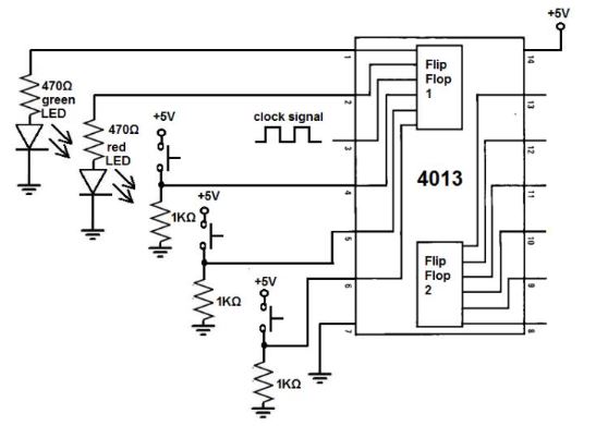
Diagram of CD4013
To achieve smooth performance of the CD4013, it's advisable to carefully connect VDD and GND to their respective power terminals. The device operates within a voltage range of 3V to 15V, and some models extend up to 20V. Reference the specific datasheet to determine these capabilities. Considerations regarding power supply play a role in integrating the CD4013 into various electronic frameworks. Data input through the D pin stays dormant until a decisive trigger—a transition from LOW to HIGH—activates at the CLK pin.

• The D (data) pin is where you input the data you want to store in the flip-flop.
• Provide a signal that goes from LOW to HIGH on the CLK pin to store the data from the D pin to the output pin Q.
• The output pin Q is always the opposite of pin Q.
• Use the S (set) pin to force the output pin HIGH.
• Use the R (reset) pin to force the output pin LOW.
CD4013 Substitute Models
• 4174: Hex D-type Flip-Flop
• 4175: Quad D-type Flip-Flop
• 40174: Hex D-type Flip-Flop
• 40175: Quad D-type Flip-Flop
• 74HC74: Dual D-type Flip-Flop
• 74HC79: Dual D-type Flip-Flop
CD4013 Dimensions

CD4013 Manufacturer
On Semiconductor, listed on Nasdaq as ON, is dedicated to enhancing energy-efficiency through its diverse range of power and signal management, logic, and customized solutions. It boasts robust supply chain capabilities complemented by a network of high-reliability manufacturing facilities, sales offices, and design centers located strategically across North America, Europe, and the Asia Pacific, catering to markets.
Datasheet PDF
CD4013BCM Datasheets
CD4013BCM.pdfCD4013BCM Details PDF
CD4013BCM PDF - DE.pdf
CD4013BCM PDF - FR.pdf
CD4013BCM PDF - ES.pdf
CD4013BCM PDF - IT.pdf
CD4013BCM PDF - KR.pdf
function test. The highest cost-effective products and the best service is our eternal commitment.
Hot Article
- LM358 Dual Operational Amplifier Comprehensive Guide: Pinouts, Circuit Diagrams, Equivalents, Useful Examples
- Are CR2032 and CR2016 Interchangeable?
- Understanding the Differences ESP32 and ESP32-S3 Technical and Performance Analysis
- BC547 Transistor Basics: Pinout, Application Circuits, Alternative/Complementary Models
- Choosing the Right Battery: A Guide to AG4, LR626, LR66, 177/376/377, SR626, and SR626SW Equivalents
- NPN vs. PNP: What's the Difference?
- esp32 vs stm32: which microcontroller is better for you?
- What Is a MOSFET and How It Works?
- Electrical Relay Basic: Working Operation, Types and Uses
- PNP Transistors: Structure, Working Principle and Application
 J111 JFET Transistor Guide
2024-11-07
 Comprehensive Guide into STM32F446ZET6 Microcontroller
2024-11-07
Frequently Asked Questions [FAQ]
1. How Does CD4013 Work?
The 4013 encompasses two separate D-type flip-flops with asynchronous set/reset inputs. When the set or reset terminals are activated by a high signal, the respective output is instantly updated. Conversely, both outputs mirror the input data from the last low-to-high clock edge whenever set and reset signals are low.
2. What is CD4013 Used For?
Known as the CD4013 or IC-4013, this CMOS logic chip integrates two D-Type (DATA) Flip-flops. The D input data is retained when a clock pulse reaches the clock pin, C. By connecting the clock and both Q outputs, we can create a toggle flip-flop suitable for counting applications.
3. What is a Clock Signal in Flip-Flops?
A clock pulse refers to a time-varying voltage signal that governs the operation, or triggering, of a flip flop. To illustrate, a clock pulse with a frequency of 1 Hz applies voltage that fluctuates between specific values, X Volts and Y Volts, at intervals of half a second.
4. What Happens if a Flip-Flop has No Clock?
Flip flops serve as memory units, with clocks enabling them to list responses to external stimuli. Changes at the input only register when the clock is active. Thus, if the clock is indefinitely disabled, the flip flop will perpetually hold the prior input state.
5. Is a D Flip-Flop Edge-Triggered?
Indeed, the D flip-flop functions as an edge-triggered device, transferring input data to the Q output during a clock's rising or falling edge. While data latches and transparent latches are regarded as level-sensitive devices, the D flip-flop responds distinctly to edge transitions.
Hot Part Number
 V300A48M500BL
 T510E108M004AS4115
 S912B32E4VFUE8R
 TAJD108M002RNJ
 C3216X7S0G476M160AB
 T491D106M035AT7128
 GRM0336R1E1R2CD01D
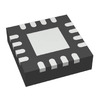 TPS2541RTET
 CGA9N3X7S2A106K230KB
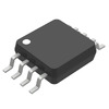 NCV2903DMR2G
- CL05B562KA5NNNC
- GQM2195C1H470GB01D
- CL10C151GB8NNWC
- CAT3200ZI-GT3
- ADG721BRMZ-REEL
- 843252AGLFT
- AD9226ARSZRL
- EP1S25F1020C5
- VI-JT3-EW
- LP2953IM-3.3
- F6KA2G605A4LA-Z
- 1206PC473KAT2A
- LAN9514-JZX-TR
- CGA3E3X8R2A333M080AD
- RTC-72421B
- V48C12C150B
- GRM1885C2A8R0DA01J
- LC898212XD-SH
- XRT86VX38IB256-F
- GCM1555C1H391JA16D
- ADS8341EB
- 6MBI35S-140-50
- ADF4106BRUZRL
- ATAR862N-087-TNQ38
- BCM5751MKFBG
- BQ20881DBTR
- EL2120CS
- K4B4G1646E-BCK0
- M5M5V108DKV-70HI
- MC14051BCP
- MPC993FA
- PI3HDMI2410-AFFE
- XCS20XL5TQ144C
- APA2621RI-TRG
- DS24B33S+T&R
- IDT71V321L25TFI
- RTL8366S-VS-GR
- SKKT215/16E
- EXO-3C16MHz