Learn How JK Flip-Flops Work and Where They Are Used in Digital Circuits
2025-10-17
8997
Catalog
Understanding the JK Flip-Flop
A JK flip-flop is a digital circuit used to store one bit of data. It’s a main building block in counters, memory units, and control systems. Like other flip-flops, it changes state based on a clock (CLK) signal, which determines when the output updates. The JK flip-flop improves on the simpler SR latch by eliminating its invalid state. It uses two inputs, J and K, and a clock input. The J and K signals control whether the output Q is set, reset, held, or toggled. The name JK doesn’t describe what the inputs do it was chosen to distinguish this design from earlier ones. Most sources attribute the name to Jack Kilby, who developed the circuit concept.
The JK flip-flop only changes its output when the clock is active. Its behavior depends on the combination of J and K values:
|
CLK |
J |
K |
Next
Q |
Operation |
|
0 |
X |
X |
Q |
No change |
|
1 |
0 |
0 |
Q |
Hold (Memory) |
|
1 |
1 |
0 |
1 |
Set |
|
1 |
0 |
1 |
0 |
Reset |
|
1 |
1 |
1 |
Q̅ |
Toggle |
• Set: When J = 1 and K = 0, the output becomes 1.
• Reset: When J = 0 and K = 1, the output becomes 0.
• Hold: When J = K = 0, the output remains the same.
• Toggle: When J = K = 1, the output flips to its opposite state.
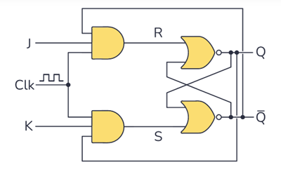
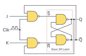
Figure 2. JK flip-flop built using NAND gates and an SR (Set-Reset) latch
The JK flip-flop’s ability to toggle makes it especially useful for binary counting and frequency division. It is built from logic gates, typically NAND or NOR gates, arranged around a basic SR latch. The outputs feed back into the input gates, allowing the circuit to toggle when both J and K are high, which makes the JK flip-flop more flexible than the SR latch. However, in a level-triggered JK flip-flop, if the clock stays high while both J and K are 1, the output can switch rapidly between 0 and 1 before the clock goes low. This unwanted oscillation is known as the race-around problem.
Understanding the JK Flip-Flop Symbol
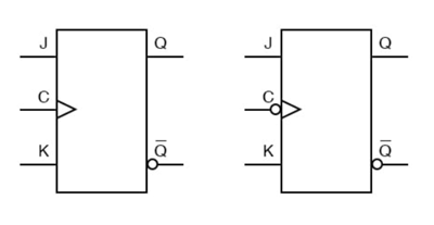
Figure 3. JK flip-flop Symbols
The JK flip-flop has two main inputs, J and K, and two outputs, Q and Q̅. It also includes a clock input (CLK) with an edge indicator that shows whether it responds to the rising or falling edge of the clock signal. Some versions include optional Preset (PRE/SET) and Clear (CLR/R) inputs for asynchronous control, allowing the output to be set or reset instantly, independent of the clock.
A triangle on the clock input (CLK) indicates a positive-edge triggered flip-flop, meaning it updates when the clock signal transitions from 0 to 1. A triangle with a bubble represents a negative-edge triggered flip-flop, which updates when the clock signal goes from 1 to 0. The bubble on the Preset (PRE) or Clear (CLR) input shows that the input is active low. To interpret the symbol correctly, first identify the clock edge marker, then check the PRE and CLR inputs, and finally relate the J and K inputs to the truth table for the correct operation.
Types of JK Flip-Flops
1. Pulse-Triggered (Master-Slave) JK Flip-Flop
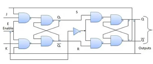
Figure 4. Master–Slave JK Flip-Flop Circuit Diagram
A pulse-triggered JK flip-flop is a variation of the standard JK flip-flop that updates its output only after a complete clock pulse. It uses the master–slave configuration to eliminate the race-around problem, ensuring stable and predictable output transitions.
A pulse-triggered JK flip-flop consists of two latches connected in series:
• The master latch captures input values (J and K) when the clock (CLK) is high.
• The slave latch updates the final output (Q) when the clock goes low.
This sequence ensures that only one output change occurs per full clock pulse, making the circuit more stable and reliable.
How the Master–Slave Setup Works?
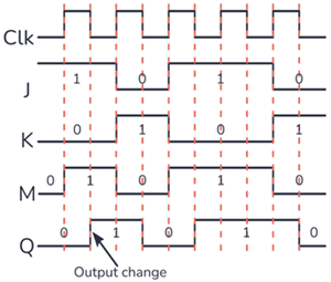
Figure 5. Timing Diagram of a Pulse-Triggered (Master-Slave)
Here’s what happens step by step:
• Rising Edge (0 → 1): The master latch becomes active. It reads the J and K inputs and updates its internal state accordingly.
• Clock High: While the clock remains high, the slave latch stays inactive, holding the previous output state.
• Falling Edge (1 → 0): The clock inversion activates the slave latch, transferring the master’s stored state to the output Q.
The output changes only after a complete clock cycle (0 → 1 → 0). This controlled behavior gives the circuit its name: pulse-triggered JK flip-flop.
Truth Table of a Pulse-Triggered JK Flip-Flop
|
Clock
Pulse |
J |
K |
Next
Q |
Operation |
|
0 or 1 (no full pulse) |
X |
X |
Q |
No change |
|
0 → 1 → 0 |
0 |
0 |
Q |
Memory (Hold) |
|
0 → 1 → 0 |
1 |
0 |
1 |
Set |
|
0 → 1 → 0 |
0 |
1 |
0 |
Reset |
|
0 → 1 → 0 |
1 |
1 |
Q̅ |
Toggle |
Each action occurs only once per full clock pulse, preventing multiple toggles during a single clock period.
The master–slave JK flip-flop offers stable and reliable operation by preventing the race-around problem its output changes only once per clock pulse, even when both inputs are high. By separating input capture and output update, it avoids glitches and ensures accurate timing, making it ideal for counters and control circuits. To work properly, inputs (J and K) must remain steady around the clock edge, the clock pulse must be the right width, and propagation delay through both latches must be managed to maintain speed and stability.
2. How Edge-Triggered JK Flip-Flops Work?
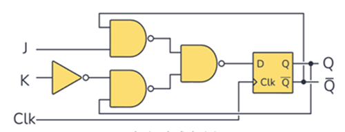
Figure 6. Edge-Triggered JK flip-flop
An edge-triggered JK flip-flop is a type of digital circuit that changes its output only at a specific clock transition, known as an edge. Unlike the master–slave JK flip-flop, which requires a full clock pulse (0→1→0) to update, the edge-triggered version reacts instantly to a single clock transition either a rising edge (↑) or a falling edge (↓). This design improves timing accuracy and eliminates the race-around problem found in level-triggered circuits.
How Edge Triggering Works?
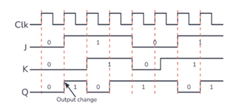
Figure 7. Operation of an edge-triggered JK flip-flop
In an edge-triggered JK flip-flop, the J and K inputs are sampled only at the moment of the clock edge. Once that edge occurs, the flip-flop updates its output (Q) based on the current input combination. Between edges, the output remains stable and unaffected by changes in J or K.
Rising-edge triggered flip-flops respond when the clock goes from low to high (0→1), while falling-edge triggered ones respond when the clock goes from high to low (1→0).
This precise timing ensures reliable performance in synchronous circuits such as counters, registers, and frequency dividers.
Truth Table of the Edge-Triggered JK Flip-Flop
|
Clock
Edge |
J |
K |
Next
Q |
Description |
|
No rising edge |
X |
X |
Q |
No change |
|
↑ (0→1) |
0 |
0 |
Q |
Hold (Memory) |
|
↑ (0→1) |
1 |
0 |
1 |
Set |
|
↑ (0→1) |
0 |
1 |
0 |
Reset |
|
↑ (0→1) |
1 |
1 |
Q̅ |
Toggle |
The output changes only at the clock edge, ensuring that Q updates once per transition. This behavior makes the JK flip-flop ideal for timing-sensitive digital systems.
An edge-triggered JK flip-flop can be made using a rising-edge D flip-flop, along with NAND and NOT gates. The signal is applied to the D flip-flop to produce JK behavior that updates only on the clock’s rising edge. This setup prevents race-around issues, provides stable and consistent output, simplifies timing control, and is widely used in integrated circuits and digital simulations for dependable performance.
JK Flip-Flop Integrated Circuits
|
IC |
Flip-Flops
per Chip |
Trigger
Type |
Special
Inputs |
Technology |
Typical
Supply |
|
CD4027 |
2 |
Positive-edge |
Set, Reset |
CMOS |
3V–15V |
|
74HC73 |
2 |
Negative-edge |
Clear |
CMOS |
2V–6V |
|
74LS73 |
2 |
Negative-edge |
Clear |
TTL |
5V |
|
74HC112 |
2 |
Negative-edge |
Preset, Clear |
CMOS |
2V–6V |
Match the supply voltage and logic family to the rest of your circuit to ensure compatibility and stable operation. Decide whether you need a rising-edge or falling-edge triggered device based on how your clock signal is designed. Consider whether your application requires only a reset input or both preset and clear functions for proper initialization. Finally, always check the setup time, hold time, and propagation delay specifications to make sure the flip-flop can handle your circuit’s intended clock frequency.
Uses of JK Flip-Flops
• Counters and frequency dividers: set J = K = 1 for toggle and chain stages for mod-N counting.
• Shift registers and data conversion: serial to parallel and parallel to serial movement of bits.
• Registers and small memory: simple storage elements for flags and control data.
• State machines and control logic: predictable set, reset, hold, and toggle behavior for sequencers.
Advantages and Disadvantages of JK Flip-Flops
Advantages
Versatile operation in one device: set, reset, hold, toggle
Natural toggle mode for divide-by-2 and counting
Available with asynchronous preset and clear
Clear educational model for sequential logic
Disadvantages
More internal logic than a D flip-flop, which increases area and delay
Level-sensitive versions can race when J = K = 1 and clock is high
Sensitive to timing if setup, hold, or pulse width are violated
Conclusion
The JK flip-flop is an important part of digital design because it’s flexible and reliable. It can work as memory, a counter, or a frequency divider in one circuit. Knowing how each type works and managing timing correctly helps you build stable and efficient system.
function test. The highest cost-effective products and the best service is our eternal commitment.
Hot Article
- LM358 Dual Operational Amplifier Comprehensive Guide: Pinouts, Circuit Diagrams, Equivalents, Useful Examples
- Are CR2032 and CR2016 Interchangeable?
- Understanding the Differences ESP32 and ESP32-S3 Technical and Performance Analysis
- Choosing the Right Battery: A Guide to AG4, LR626, LR66, 177/376/377, SR626, and SR626SW Equivalents
- BC547 Transistor Basics: Pinout, Application Circuits, Alternative/Complementary Models
- NPN vs. PNP: What's the Difference?
- esp32 vs stm32: which microcontroller is better for you?
- What Is a MOSFET and How It Works?
- Electrical Relay Basic: Working Operation, Types and Uses
- PNP Transistors: Structure, Working Principle and Application
 Understanding Pumps: Basics, Types, Specs, and Common Problems
2025-10-17
 What Is a Photodiode: Working Principles, Modes, Advantages and Applications
2025-10-17
Frequently Asked Questions [FAQ]
1. Why is the JK flip-flop called a universal flip-flop?
It’s called universal because it can perform the functions of other flip-flops like SR, D, and T types by changing the input logic conditions.
2. What happens when both J and K inputs are 0?
When J and K are both 0, the JK flip-flop holds its previous output state. No change occurs until the inputs or clock signal change.
3. How do you convert a JK flip-flop into a T flip-flop?
By connecting both J and K inputs together and setting them to logic 1, the JK flip-flop toggles its output with every clock pulse, working like a T flip-flop.
4. What is the propagation delay in a JK flip-flop?
Propagation delay is the short time it takes for the output (Q) to change after the clock or input changes. It limits the maximum speed of operation in digital circuits.
5. Can JK flip-flops be used in microcontrollers?
Not directly, but their functions are often built into microcontroller registers and timers. In hardware design, external JK flip-flops are used in logic-based timing or counting applications.
6. What logic gates are used to build a JK flip-flop?
JK flip-flops are typically built using NAND or NOR gates arranged around an SR latch, with feedback loops that allow toggling when both J and K are high.
7. How do you test a JK flip-flop in a lab circuit?
Apply a known clock signal and vary the J and K inputs. Observe the output using LEDs or an oscilloscope to confirm set, reset, hold, and toggle operations.
Hot Part Number
 C1608X7R1E474K080AB
 C2012X5R0J225K085AA
 GRM0225C1E4R1CDAEL
 CC0603ZRY5V6BB474
 UMK316B7474ML-T
 08051U150GAT2A
 GRM1886S1H1R1CZ01D
 T495D476K010ATE080
 TPSE106M050R0500
 APA600-PQ208
- MT47H64M8CF-25E:G
- MC9S12XA512VAL
- IS42S16160B-6TL
- SI8233AD-D-IS
- RT0402DRD072K49L
- CY8C20140-SX2I
- VLF4012AT-100MR79
- SKM150GAL128D
- MC100ELT21DR2G
- MC14040BDTR2G
- LT3971AIMSE#PBF
- T491D107K006ZT7280
- UCC3818N
- INA240A2PW
- IXFP22N65X2M
- LT1999CMS8-50F#PBF
- SN74LVC32ADR
- AD5262BRUZ20-RL7
- ATMXT1666T2-C2U
- BU20360-48L
- ICS950218AFT
- MAX1779EUE+TG104
- MAX202ECWE-T
- MAX8860EUA27
- G5LA-1A4-12V
- HN29V256AOBBP-30
- M66445M1FA
- NFP-2200-A3
- PCD8010H/E31/4
- PEAD22653AFV1QH14NAR
- 6MBP150RTM060
- S29GL032A90FAIR43
- TMR3-1211
- T6TD7XBG-0001
- CS242C001PZ-TRSV
- IBMPPCBWY-GES72914
- SDINBDG4-8G-XI1
- XFL4020-332MEC
- GMOV-14D500K