Frequently Asked Questions
What makes the ZDT649TC suitable for switching applications that require both high frequency and moderate current handling?
The ZDT649TC integrates two independent NPN transistors in a single SM8 package, each capable of handling 2A collector current with a transition frequency of 240MHz. This combination allows designers to implement dual-channel switching circuits—such as complementary driver stages or push-pull configurations—while maintaining fast switching response. The 240MHz transition frequency ensures that the ZDT649TC can reliably switch signals in RF front-end circuits, audio amplifiers, and logic-level switching applications without introducing significant switching delays that would degrade signal integrity or reduce operational bandwidth.
How do the saturation characteristics of the ZDT649TC affect circuit design for saturated switching versus linear amplification?
The ZDT649TC exhibits a maximum Vce saturation of 500mV at 2A collector current with 200mA base current, indicating relatively strong saturation performance. This low saturation voltage means less power is dissipated as heat during the on-state, making the ZDT649TC well-suited for switching regulators, relay drivers, and load switches where efficiency matters. For linear amplification applications, the saturation characteristics constrain headroom; designers must ensure that the ZDT649TC operates in the active region rather than deep saturation to maintain predictable gain (minimum hFE of 100 at 1A, 2V) and avoid storage time delays during switching transitions.
What are the thermal design considerations when using the ZDT649TC in circuits dissipating near its 2.75W maximum power rating?
The ZDT649TC's 2.75W maximum power dissipation assumes adequate thermal coupling to the PCB and ambient cooling. At full rated power, the junction temperature can reach 150°C (the upper operating limit) if the ambient exceeds approximately 80–90°C, depending on PCB copper area and thermal vias. Designers implementing the ZDT649TC in applications such as motor drivers or high-frequency power amplifiers should calculate worst-case power dissipation (P = Ic × Vce + Ib × Vbe) and plan thermal management accordingly. Inadequate heat sinking can cause the ZDT649TC to self-limit via temperature rise, reducing available gain and switching speed.
Why is the dual-transistor configuration of the ZDT649TC preferable to using two discrete single transistors in compact switching applications?
The ZDT649TC's integrated dual-transistor design in an SM8 package reduces PCB footprint compared to two separate SOT-23 or SOT-89 packages, lowering assembly cost and improving circuit density in space-constrained applications. The matched characteristics between the two transistors within the ZDT649TC—fabricated on the same die with identical processing—provide better matching of hFE, Vbe, and switching speed than individually sourced components. This matching is valuable in balanced driver stages, differential amplifiers, and push-pull output circuits where tracking between channels affects linearity and distortion. The single-package approach also simplifies thermal management by concentrating heat at one point on the PCB.
How does the ZDT649TC's collector cutoff current (ICBO) specification influence circuit behavior in high-impedance or sensor interface applications?
The ZDT649TC specifies a maximum ICBO (collector-base leakage current) of 100nA, which represents a relatively modest leakage floor. In high-impedance sensor circuits or precision signal conditioning stages, leakage current from the ZDT649TC's base-collector junction can introduce offset errors or bias instability if the source impedance exceeds several megohms. Designers using the ZDT649TC as an input buffer for low-level analog signals should include appropriate biasing resistors (typically 1–10 kΩ) to swamp the leakage effect and maintain stable quiescent conditions. At elevated temperatures approaching 150°C, ICBO can rise significantly, so thermal margin calculations are necessary for precision applications.
What design trade-offs exist between using the ZDT649TC versus a dedicated integrated switch or MOSFET for a 2A load switching application?
The ZDT649TC offers advantages in circuits requiring base-drive control and relatively low operating voltages (up to 25V VCEO). Compared to a MOSFET, the ZDT649TC's bipolar architecture requires continuous base current to maintain saturation (typically 20% of collector current), which adds power dissipation in the driver circuit but allows simpler level-shifting and current-source driving. The ZDT649TC's 500mV saturation voltage is significantly higher than a comparable low-Rdson MOSFET, resulting in greater conduction losses at high duty cycles. However, the ZDT649TC excels when matched-pair performance, high-frequency switching (240MHz transition frequency), or base-drive flexibility is needed. For DC load switching at low frequencies and high efficiency, MOSFETs generally consume less power; for RF or audio applications leveraging the ZDT649TC's 240MHz bandwidth, bipolars often provide superior performance per unit area.
How does the temperature coefficient of hFE in the ZDT649TC affect biasing stability across the -55°C to 150°C operating range?
The ZDT649TC's DC current gain (hFE) minimum of 100 at 1A, 2V is specified at a nominal temperature; hFE typically increases by approximately 0.5% per °C across the operating range. This positive temperature coefficient means that at 150°C junction temperature, hFE can increase by 50–75% relative to room-temperature values, causing base current to decrease if circuit biasing is fixed. In switching applications, rising hFE improves switching efficiency (lower base drive required), but in linear amplifiers or current sources where stable gain is critical, the ZDT649TC requires temperature-compensated biasing. Using emitter degeneration resistors (typically 10–100 Ω) or current-mirror bias networks with the ZDT649TC can maintain stable operating points across the temperature range.
Is the ZDT649TC appropriate for automotive electronics, and what environmental or reliability considerations apply?
The ZDT649TC is rated for -55°C to 150°C junction temperature, which overlaps automotive ambient ranges, but suitability depends on the specific application. The ZDT649TC is RoHS3 compliant and REACH affected, meeting EU environmental standards applicable to automotive suppliers. However, the ZDT649TC is not explicitly qualified to automotive-grade AEC-Q standards (such as AEC-Q200 for discrete semiconductors); designers targeting automotive body electronics or infotainment systems should verify with the manufacturer whether the ZDT649TC meets the required qualification, temperature cycling, or electromigration standards. For non-safety-critical applications like window motors, sunroof control, or HVAC drivers, the ZDT649TC's thermal and electrical ratings are generally adequate; for safety-critical functions (brake control, steering), qualified components with formal AEC certification are preferred.
What practical circuit configurations exploit the 240MHz transition frequency of the ZDT649TC in RF or audio signal path applications?
The ZDT649TC's 240MHz fT (transition frequency) enables its use as a low-noise preamplifier stage, RF buffer, or intermediate-frequency (IF) amplifier in frequency bands up to the VHF range. Common-emitter or common-collector (follower) configurations using the ZDT649TC can amplify narrowband signals in the 1–100 MHz range with reasonable gain and minimal phase distortion. Audio designers implement the ZDT649TC in high-frequency boost circuits (treble emphasis) or as a driver for high-impedance loads where the transistor's gain and 240MHz bandwidth prevent rolloff within the audible spectrum. The ZDT649TC's low collector-base capacitance (typical 1–2 pF) contributes to flat gain response across audio and low-RF bands, making it suitable for precision preamps where feedback networks demand predictable high-frequency behavior.
How do the maximum ratings and safe operating area (SOA) of the ZDT649TC constrain design choices in high-current pulse applications?
The ZDT649TC's maximum ratings—2A continuous collector current, 25V VCEO, 2.75W power dissipation—define the boundary of safe operation. During pulse transients, designers must ensure that peak current and instantaneous power dissipation remain within the ZDT649TC's SOA curve, which typically permits brief excursions above continuous ratings. For example, a 5A, 100µs pulse may be sustainable if the duty cycle is low enough that average power remains below 2.75W and junction temperature stays within 150°C. However, repeated pulsing or long pulse widths can cause thermal accumulation, reducing headroom. Applications such as solenoid drivers or PWM motor control require SOA analysis to prevent latch-up or thermal runaway; designers should consult the ZDT649TC datasheet SOA graph and apply derating factors for worst-case ambient temperature.
What are the packaging and reliability implications of the ZDT649TC's SM8 (SOT-223-8) form factor for high-volume consumer electronics?
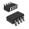
The ZDT649TC's SM8 package (SOT-223-8) is a standard surface-mount form factor widely supported by PCB fabricators and assembly equipment, making high-volume production feasible with low per-unit cost. The package's Moisture Sensitivity Level (MSL) rating of 1 (unlimited) means the ZDT649TC has no reflow-induced moisture absorption risk, simplifying storage and handling; no dry-bake or moisture-barrier packaging is required. The small footprint reduces thermal resistance to the PCB, improving heat dissipation compared to larger packages. From a reliability perspective, the SM8 package's gull-wing leads and standardized standoff height ensure consistent solder joint formation via reflow, reducing field-failure risk due to contact corrosion or thermal cycling fatigue compared to legacy through-hole designs. The ZDT649TC's ROHS3 compliance and lead-free solder compatibility are standard for modern consumer products.
How should designers handle base-emitter overvoltage protection in circuits using the ZDT649TC with inductive loads or transient spikes?
The ZDT649TC's base-emitter junction has a maximum reverse bias rating of approximately 5–7V before junction breakdown occurs. Inductive load switching—such as relay coils or motor windings driven through the ZDT649TC—can generate transient voltage spikes that exceed the supply voltage when the transistor switches off. If a clamping diode is not provided across the inductive load, the back-EMF can reverse-bias the ZDT649TC's base-emitter junction, causing damage. Standard practice is to place a fast-recovery or Schottky diode across the load (cathode to the collector of the ZDT649TC, anode to ground for a grounded emitter) to clamp the inductive transient to approximately one diode drop above the supply rail. Additionally, a base-emitter resistor (1–10 kΩ) can limit base overvoltage if the driver circuit is capacitively coupled or subject to ringing.
Why might designers choose the ZDT649TC over a single larger-current transistor when implementing parallel switching stages?
In applications requiring currents exceeding 2A—such as power amplifiers or high-brightness LED drivers—designers can connect two ZDT649TC pairs in parallel by sharing base and collector nodes. The matched hFE characteristics of the ZDT649TC's internal transistor pair improve current sharing between parallel stages compared to individually sourced devices. Each transistor within the ZDT649TC shares thermal coupling on the same die, reducing thermal runaway risk when transistors are paralleled; unmatched thermal characteristics in separately sourced transistors can cause current hogging and premature failure. By using two ZDT649TC devices in parallel (four total transistors), designers achieve 4A capability while maintaining better current distribution and thermal balance than using a single 4A transistor with potentially poorer heat dissipation or matching characteristics.
What are the frequency response and gain characteristics of the ZDT649TC in a typical common-emitter amplifier configuration?
In a common-emitter configuration, the ZDT649TC provides voltage gain approximately equal to gm × Rc (transconductance × collector load resistance). With a 2V Vce and 1A Ic, typical forward transconductance (gm) is around 40 mS (40 mA/V), so a 100Ω collector load yields approximately 4 V/V of voltage gain; higher load resistances increase gain but reduce bandwidth. The ZDT649TC's 240MHz fT, combined with typical base-collector capacitance of 1.5 pF, produces a -3dB bandwidth of roughly 10–50 MHz depending on circuit impedances and feedback networks. Input impedance at 1 mA emitter current is typically 2.5 kΩ, useful for matching to medium-impedance signal sources. When the ZDT649TC operates at lower collector currents (100 mA range), gain and bandwidth both degrade slightly due to reduced gm, but noise figure generally improves, making the ZDT649TC suitable for preamplifier stages.
How does the ZDT649TC's minimum hFE specification affect base drive design in worst-case scenarios?
The ZDT649TC specifies a minimum DC current gain (hFE) of 100 at 1A collector current and 2V Vce. In saturation, effective hFE can drop to 50–80 (forced beta), meaning base current must be at least Ic / 100 ≈ 20 mA at rated collector current to ensure adequate saturation. Design practice typically applies a base overdrive factor of 2–5×, requiring base current of 40–100 mA to force the ZDT649TC deep into saturation and minimize storage time during switching transitions. Low-impedance base drives (1 kΩ or less from the drive source) are necessary; high base impedance can result in insufficient base current during transients, causing incomplete switching and excess power dissipation in the ZDT649TC. Temperature compensation is also critical: at 150°C junction temperature, minimum hFE can increase to 150–200, reducing base drive requirements, but designers must size base resistors for worst-case cold temperature (-55°C) where hFE may drop below 100.