Frequently Asked Questions
What are the key voltage and current ratings of the ISL9V2040D3S, and how do these specifications influence circuit design decisions in switching applications?
The ISL9V2040D3S is rated for a maximum collector-emitter breakdown voltage of 430 V and a maximum collector current of 10 A, with a maximum power dissipation of 130 W. These ratings define the operating envelope for the device. The 430 V rating allows the ISL9V2040D3S to operate in industrial AC mains circuits (typically up to 400 V peak in three-phase systems) with adequate margin. The 10 A collector current limit determines the load-switching capacity; circuits requiring higher current must use multiple ISL9V2040D3S devices in parallel or select a device from a higher-current series. The 130 W power rating reflects the thermal capacity under continuous switching, which directly affects heat sink selection and thermal management strategy in the final design.
How does the Vce(on) specification of the ISL9V2040D3S affect conduction losses and thermal design?
The ISL9V2040D3S exhibits a maximum Vce(on) of 1.9 V at 4 V gate drive and 6 A collector current, measured under the specified test condition. This on-state voltage drop directly contributes to conduction loss according to Ploss = Vce(on) × Ic. At nominal switching current, this translates to approximately 11.4 W of conduction loss for the ISL9V2040D3S. For applications operating at the full 10 A rating, conduction losses could approach 19 W, requiring substantial heat sinking. Lower Vce(on) values reduce thermal stress and allow smaller heat sinks; therefore, applications with marginal thermal headroom should prioritize devices with lower on-state voltage. The test conditions for the ISL9V2040D3S (4 V gate drive, 6 A collector current) represent moderate activation conditions; actual performance may differ at higher gate overdrive or higher collector currents.
What is the significance of the 12 nC gate charge specification for the ISL9V2040D3S in high-frequency switching circuits?
The ISL9V2040D3S carries a gate charge rating of 12 nC, which represents the total electric charge required to drive the device from off-state to on-state and saturate the gate. Gate charge directly affects the switching losses and the driver circuit design. A 12 nC gate charge is relatively low for a 10 A, 430 V IGBT, allowing the ISL9V2040D3S to switch efficiently at moderate to high frequencies (typically 10–50 kHz in industrial applications) without excessive driver power dissipation. Higher gate charge would require a more robust or higher-current gate driver, increasing system complexity and cost. For the ISL9V2040D3S, a standard gate driver with 2–3 A output capacity is typically adequate, making the device suitable for compact, cost-conscious designs where driver simplicity is valued.
How does the turn-off delay (Td(off) = 3.64 µs) of the ISL9V2040D3S affect the design of bootstrap circuits and gate drive timing in switching converters?
The ISL9V2040D3S turn-off delay of 3.64 µs (measured at 25°C under the specified test conditions: 300 V, 1 kΩ, 5 V) defines the minimum time between gate signal removal and complete device turn-off. This parameter is critical in half-bridge and full-bridge topologies where dead-time insertion prevents shoot-through (simultaneous conduction of high-side and low-side switches). For the ISL9V2040D3S, dead-time must exceed 3.64 µs plus any propagation delays in the gate driver circuit; typical dead-time settings range from 5–10 µs to ensure safe margin. The turn-off delay also affects the transition edge in phase-shifted PWM designs, influencing zero-voltage-switching (ZVS) timing. Applications requiring sub-microsecond switching precision or very high frequency operation (>100 kHz) may experience timing challenges with the ISL9V2040D3S; lower-delay devices should be considered for such applications.
Is the ISL9V2040D3S suitable for automotive or automotive-grade reliability requirements?
The ISL9V2040D3S does not carry automotive qualification (AEC-Q101 or equivalent). The device is classified under ECCN EAR99 and carries an HTSUS code 8541.29.0095, consistent with industrial and consumer-grade semiconductor classification. For safety-critical automotive applications requiring fault tolerance or high reliability standards, the ISL9V2040D3S is not recommended. However, the ISL9V2040D3S may be acceptable in non-safety-critical automotive subsystems (e.g., infotainment power supplies, convenience lighting, non-essential motor drives) where industrial-grade reliability and standard commercial operation temperature range (-40°C to 175°C junction temperature) meet design requirements. Users requiring automotive-qualified IGBTs should consult onsemi's automotive-grade portfolio. The ISL9V2040D3S is optimized for industrial power conversion, renewable energy inverters, and consumer-grade switched-mode power supplies where cost and integration take precedence over automotive qualification.
What factors should be considered when selecting between the ISL9V2040D3S and alternative 10 A, 430 V IGBTs from other manufacturers?
When comparing the ISL9V2040D3S against competing devices, key differentiation factors include gate charge (12 nC for the ISL9V2040D3S is competitive but not class-leading), Vce(on) characteristics (1.9 V is mid-range for this class), switching speed (Td(off) = 3.64 µs is moderate), and cost. The ISL9V2040D3S belongs to onsemi's EcoSPARK® series, which emphasizes integration, thermal performance, and industrial reliability rather than cutting-edge switching speed. If the application prioritizes switching frequency (>50 kHz with low losses), alternative devices with lower Vce(on) (<1.5 V) or faster switching may reduce system losses. If the application is cost-sensitive and operates at moderate switching frequencies (10–25 kHz), the ISL9V2040D3S offers competitive performance per dollar. Thermal package characteristics (the ISL9V2040D3S uses TO-252AA / DPAK) should be matched against available heat sinking; alternatives in larger packages (e.g., TO-247) may be preferable for high-power designs where thermal resistance becomes limiting.
How does the TO-252AA surface-mount package of the ISL9V2040D3S affect thermal management and circuit board layout?
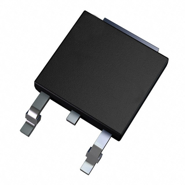
The ISL9V2040D3S employs a TO-252AA (DPAK) surface-mount package, which offers moderate thermal performance relative to larger packages. The DPAK leadframe includes a central tab for solder attachment to the PCB ground or heat-spreading layer, reducing junction-to-case thermal resistance compared to leaded packages. For the ISL9V2040D3S operating at 130 W continuous dissipation, the DPAK thermal path is often insufficient without auxiliary heat sinking; a small aluminum or copper heat sink bonded to the tab is typically required. PCB layout for the ISL9V2040D3S should emphasize a wide, thick copper layer beneath and around the tab to spread heat into the board plane, reducing local hot spots. The compact DPAK footprint allows dense board layouts, making the ISL9V2040D3S attractive for space-constrained applications. However, if sustained operation near maximum power (>100 W) is required, alternative larger packages (e.g., TO-247, module formats) should be considered to reduce thermal resistance and heat sink size.
What is the role of the ISL9V2040D3S gate input type specification, and how does it affect gate driver circuit design?
The ISL9V2040D3S carries a logic-level input specification, meaning the device is optimized for direct drive from standard TTL/CMOS logic signals (typically 0–5 V or 0–3.3 V). The gate charge of 12 nC and the test condition of 4 V gate overdrive indicate that the ISL9V2040D3S requires approximately 4–5 V above the emitter potential to achieve full saturation and low Vce(on). This logic-level design simplifies gate driver design; low-cost, non-isolated gate drivers without transformer coupling or charge pumps can be used for single-switch or low-side switching applications. For high-side switching in half-bridge topologies, the ISL9V2040D3S requires a bootstrap gate driver or isolated supply to maintain the 4–5 V gate-to-emitter voltage above the switching node. The relatively modest gate drive requirement of the ISL9V2040D3S (compared to devices requiring ±15 V or higher) reduces driver component count and system cost, making it suitable for price-sensitive industrial designs.
How do the operating temperature range (-40°C to 175°C junction) and thermal characteristics of the ISL9V2040D3S constrain system design in industrial environments?
The ISL9V2040D3S operates across a junction temperature range of -40°C to 175°C, which covers most industrial and commercial temperature scenarios. The upper limit (175°C) reflects typical power IGBT thermal limits; the Vce(on) specification (1.9 V measured at 25°C) increases with junction temperature, typically by approximately 0.4–0.5% per °C. At maximum junction temperature, the ISL9V2040D3S conduction loss may increase by 15–20% compared to 25°C operation, necessitating thermal margin in loss calculations. For applications in harsh industrial environments (outdoor equipment, high-altitude installations, proximity to thermal sources), the -40°C lower limit ensures the ISL9V2040D3S remains functional during startup, though gate drive circuits and electrolytic capacitors must also be rated for these extremes. The wide temperature range of the ISL9V2040D3S makes it suitable for uncontrolled-environment industrial inverters, renewable energy converters, and traction motor drives where ambient temperature variation is significant.
What design considerations should guide the choice between the ISL9V2040D3S and lower-voltage IGBT alternatives for 48 V or 24 V industrial power conversion?
The ISL9V2040D3S is rated for 430 V breakdown voltage, which is significantly higher than required for 48 V or 24 V DC bus applications. In such applications, the excess voltage headroom of the ISL9V2040D3S introduces several trade-offs. First, the Vce(on) of the ISL9V2040D3S (1.9 V at 6 A) may be higher than optimized low-voltage devices rated for 60 V or 100 V, resulting in higher conduction losses and thermal stress for the same output power. Second, the gate charge and switching delays of the ISL9V2040D3S may not be optimal for the faster switching frequencies (>50 kHz) often employed in low-voltage converters to reduce filter size. Third, cost per watt is typically higher for the ISL9V2040D3S in low-voltage applications where lower-voltage devices are more cost-effective. However, if a single-design solution must serve multiple voltage rails (e.g., 24 V and 400 V subsystems in industrial equipment), the ISL9V2040D3S offers the flexibility to operate across this range without re-qualification. For dedicated low-voltage designs, alternatives optimized for 60–100 V operation should be evaluated.
How does the ISL9V2040D3S perform in inductive switching circuits, and what precautions are necessary for clamping and snubber design?
The ISL9V2040D3S, like all IGBTs, exhibits reverse-recovery characteristics when switching inductive loads. During turn-off transients, stored minority carriers create a reverse current spike before the device blocks completely, temporarily reducing Vce to near zero. In high-inductance circuits, this reverse recovery can create voltage overshoot as the collector-emitter voltage rebounds; uncontrolled, these spikes can exceed the 430 V rating of the ISL9V2040D3S and cause failure. Design practices for the ISL9V2040D3S in inductive switching include: (1) connecting a fast recovery diode (or antiparallel diode) across the collector-emitter terminals to conduct reverse recovery current and limit overshoot; (2) adding RC snubbers across the device to damp oscillations; (3) ensuring gate drive impedance is low to minimize turn-off transition time. The gate charge of 12 nC and turn-off delay of 3.64 µs for the ISL9V2040D3S suggest moderate switching speed; additional snubbing may be necessary in switching frequencies exceeding 50 kHz with high inductive loads. The ISL9V2040D3S is therefore best suited to applications where inductive energy is predictable (motor drives, transformer-coupled circuits) rather than unpredictable load transients.
What lifetime and reliability considerations apply to the ISL9V2040D3S in continuous industrial operation?
The ISL9V2040D3S carries moisture sensitivity level MSL 1 (Unlimited), indicating excellent moisture resistance and storage stability across industrial and commercial supply chains. This classification reduces moisture bake-out requirements and supports standard assembly processes. For long-term reliability, the ISL9V2040D3S is subject to degradation mechanisms common to IGBTs: (1) gate-oxide wearout under high electric fields or high-temperature bias, typically accelerated by gate voltages significantly exceeding the specified 4–5 V range; (2) aluminum wire bond fatigue under thermal cycling, affecting devices subjected to repetitive temperature swings >50°C; (3) junction leakage growth at elevated temperatures, which increases with time and temperature according to an Arrhenius model. The ISL9V2040D3S is not formally rated for mean-time-between-failures (MTBF) under industrial standards, but typical design life in controlled industrial environments (temperature cycling <30°C, no mechanical vibration) exceeds 10 years. Applications requiring quantified reliability (e.g., safety systems, mission-critical equipment) should employ redundancy or derating strategies, operating the ISL9V2040D3S significantly below maximum ratings (e.g., <50% voltage, <50% current, <100°C junction) to extend lifetime.
How does the EcoSPARK® series positioning of the ISL9V2040D3S influence its performance and cost trade-offs compared to competing IGBT series?
The ISL9V2040D3S belongs to onsemi's EcoSPARK® series, which emphasizes cost-to-performance balance for industrial and renewable energy applications rather than cutting-edge performance optimization. The EcoSPARK® positioning of the ISL9V2040D3S reflects design choices favoring: (1) robust Vce(on) and switching characteristics at moderate speeds (suitable for 10–50 kHz operation), (2) simplified gate drive requirements and good thermal integration in compact packages, (3) competitive cost per watt for volume production. Compared to performance-optimized series with lower Vce(on) or faster switching, the ISL9V2040D3S typically costs 15–30% less in high volumes but operates with slightly higher total switching losses. Compared to lower-cost commodity IGBTs, the ISL9V2040D3S offers superior integration, reliability, and thermal performance. The EcoSPARK® positioning makes the ISL9V2040D3S well-suited to price-sensitive mass-production applications (e.g., grid-tied solar inverters, industrial motor drives, switched-mode power supplies) where 5–10% system efficiency differences are acceptable and cost competition is intense.
What gate drive circuit components and ratings are recommended to safely operate the ISL9V2040D3S at its maximum rated power and switching frequency?
To safely operate the ISL9V2040D3S at or near maximum specifications (10 A collector current, 130 W dissipation, 50 kHz switching frequency), gate drive design should incorporate: (1) a dedicated gate driver IC with 2–3 A peak output current (e.g., IR2110, TL494, or equivalent) to rapidly charge and discharge the 12 nC gate charge within acceptable rise/fall times; (2) a gate resistor (typically 5–10 Ω for the ISL9V2040D3S) to limit dI/dt and EMI while maintaining adequate switching speed; (3) a resistor from gate to emitter (typically 10 kΩ) to ensure the ISL9V2040D3S remains off during power-up or signal loss; (4) a bootstrap capacitor (10–47 µF) if high-side switching is required, rated for at least 25 V. The ISL9V2040D3S gate drive power supply should be rated for 12–15 V (or ±15 V for bidirectional operation) to provide adequate overdrive margin above the 4 V saturation threshold. Circuit simulations or experimental validation are recommended to confirm that dV/dt during switching (influenced by transformer coupling and snubber design) does not cause spurious gate triggering.
How should the ISL9V2040D3S be compared against MOSFETs in the same voltage and current class for switching applications?
The ISL9V2040D3S is an IGBT, not a MOSFET, and the choice between the two device types involves significant trade-offs. Compared to power MOSFETs rated for 430 V and 10 A, the ISL9V2040D3S exhibits lower Vce(on) (1.9 V) than high-voltage MOSFETs (which typically exhibit Rds(on) > 10 Ω, yielding conduction voltage > 3 V at 6 A), resulting in lower conduction losses for the ISL9V2040D3S in moderate-current applications. However, MOSFETs generally exhibit faster switching times and lower gate charge (often <5 nC) compared to the ISL9V2040D3S (12 nC), enabling higher switching frequencies (>100 kHz) with lower switching losses. MOSFETs also eliminate reverse-recovery losses, simplifying snubber design. For the ISL9V2040D3S, the advantage lies in cost-per-watt at moderate switching frequencies (10–50 kHz) and in applications where gate drive simplicity is valued. The choice between the ISL9V2040D3S and MOSFETs should be based on system efficiency targets, switching frequency, thermal budget, and cost at the planned production volume.
What are the typical failure modes of the ISL9V2040D3S, and how should circuit design mitigate them?
Common failure modes of the ISL9V2040D3S in field applications include: (1) gate oxide rupture due to excessive gate-to-emitter voltage (e.g., >10 V sustained drive) or transient overvoltage spikes; (2) thermal runaway if Vce(on) increases beyond design margin due to aging or extended high-temperature operation; (3) junction short-circuit if internal metallization migrates or wire bonds fracture due to thermal cycling. For the ISL9V2040D3S, mitigation strategies include: (1) clamping gate-to-emitter voltage to ±15 V using Zener diodes or gate clamps; (2) maintaining junction temperature well below 175°C through adequate heat sinking and derating (targeting <150°C in production designs); (3) using bootstrap diodes with low forward voltage and fast reverse recovery to minimize voltage stress on the ISL9V2040D3S during high-side switching. PCB layout should minimize loop areas around the ISL9V2040D3S gate and collector terminals to reduce electromagnetic coupling and spurious switching. The ISL9V2040D3S should be protected against source faults (e.g., short circuits) using fast current-limiting circuits or fold-back current limiting in the gate drive to prevent catastrophic failure.